Analyzing TSMC's fab expansion roadmap — multi-fab N2 ramp, CoWoS, SoIC, and uncorking bottlenecks
Jun 10, 2026 - 16:10
01
(Image credit: Getty Images / Jimmy Beunardeau)
When we referred to TSMC just several years ago, we called it 'the world's largest foundry,' implying that Intel was still the world's largest producer of advanced logic chips. However, having spent nearly $240 billion on capacity expansion over the last 10 years, TSMC now has nine sites with dozens of 300-mm fabs, many of which can process orders of magnitude more wafers using EUV-based process technologies than Intel*, which makes TSMC the world's largest maker of advanced logic chips.
Being the world's largest maker of advanced AI processors requires TSMC to stay ahead of its rivals, Intel and Samsung Foundry, both in terms of process technologies and, perhaps, even more importantly, in terms of production capacity.
Therefore, TSMC has kicked off the most aggressive manufacturing expansion in its history as the company races to meet explosive demand for AI processors, logic chips made on leading-edge nodes, and advanced packaging.
(Image credit: TSMC)
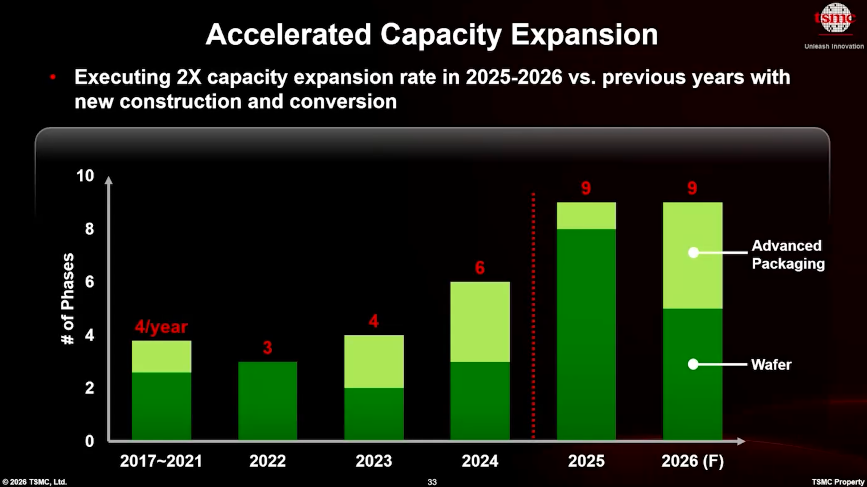
During TSMC's Tech Symposium 2026 manufacturing presentations, the company revealed that in 2025 – 2026, it effectively doubled its historical construction pace, building or converting nine fab phases annually, up from an average of four phases per year. The company is simultaneously building or ramping new fabs in Taiwan, the U.S., Japan, and Germany. In addition, it introduces new ways to improve the productivity of existing facilities.
Swipe to scroll horizontally
TSMC's new or ramping production facilities
Site Name
Phase
Capabilities
Fab Location
Status
Fab 20
1, 2
A16, N2
Hsinchu, Taiwan
Ramping
Fab 21
2
N3
Phoenix, Arizona
Equipping
Fab 21
3, 4
A16, N2
Phoenix, Arizona
In construction
Fab 22
1
A16, N2
Kaohsiung, Taiwan
Ramping
Fab 22
2, 3
A16, N2
Kaohsiung, Taiwan
Equipped, ramping in H2 2026
Fab 23 - JASM
2
Down to N3
Kumamoto, Japan
In construction as of January 2025. Construction stalled.
Fab 24 - ESMC
1
N12, N16, N22, N28
Dresden, Germany
In construction as of August 2024
Fab 25
1
A14, A13, A12
Taichung, Taiwan
In construction
N2 ramp: Six-figure amounts of wafers per-month by 2029
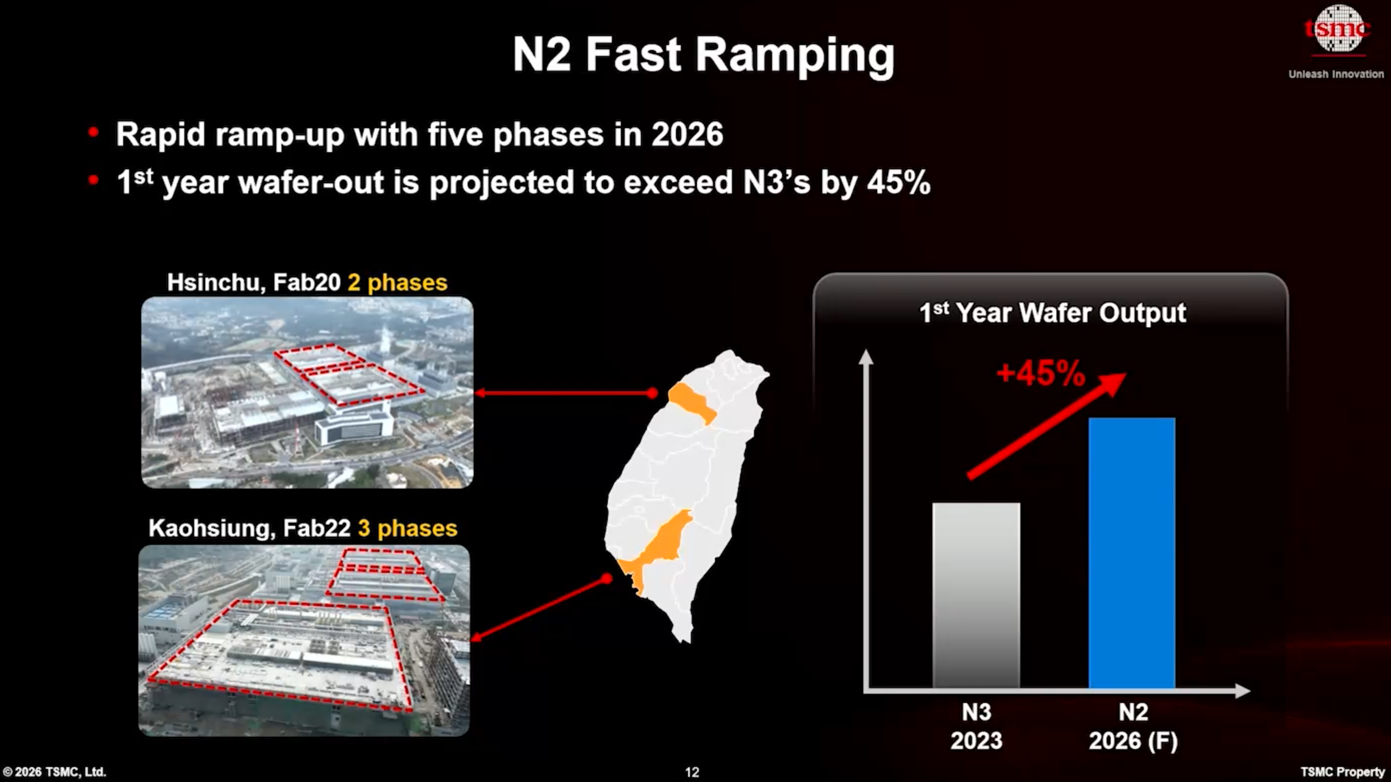
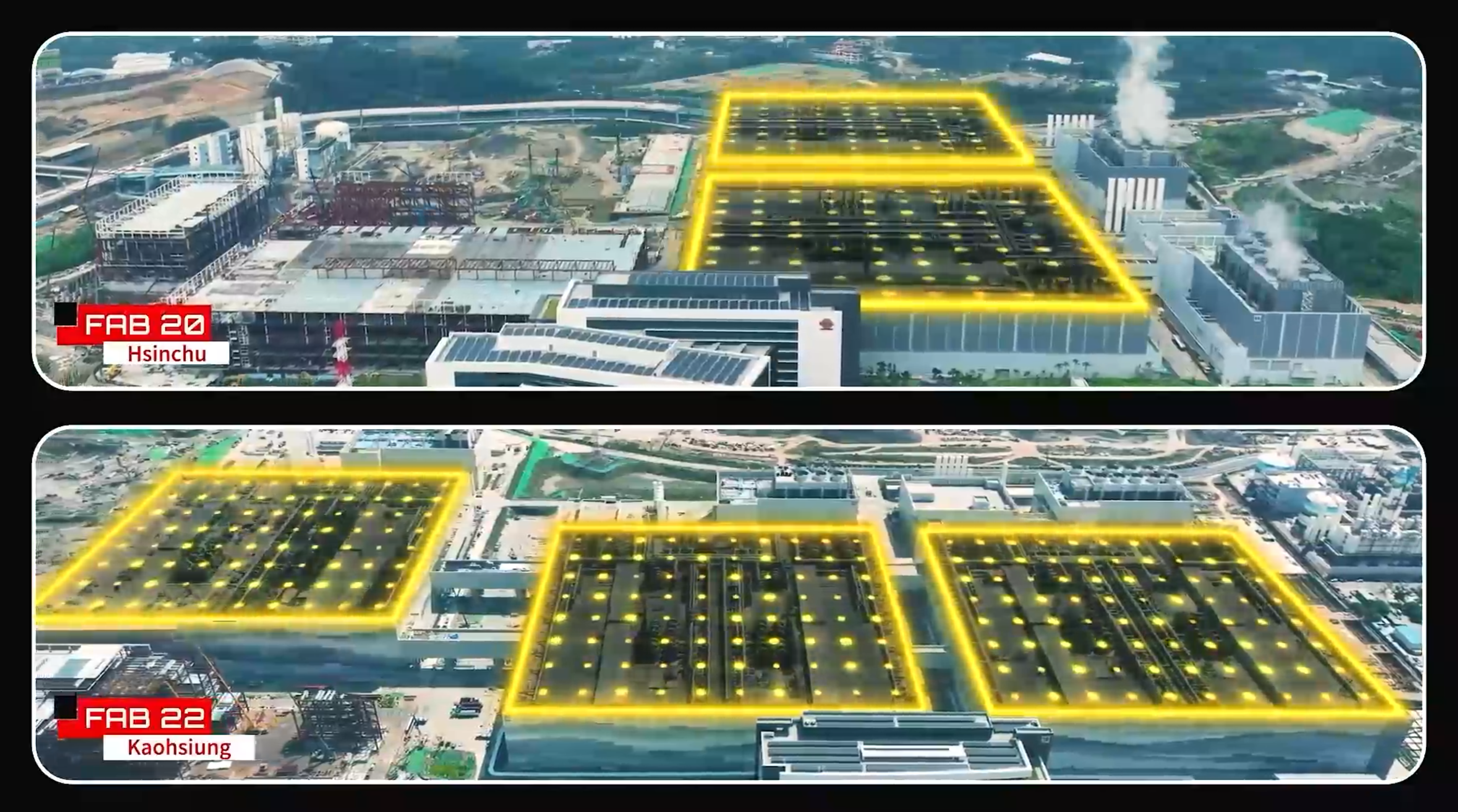
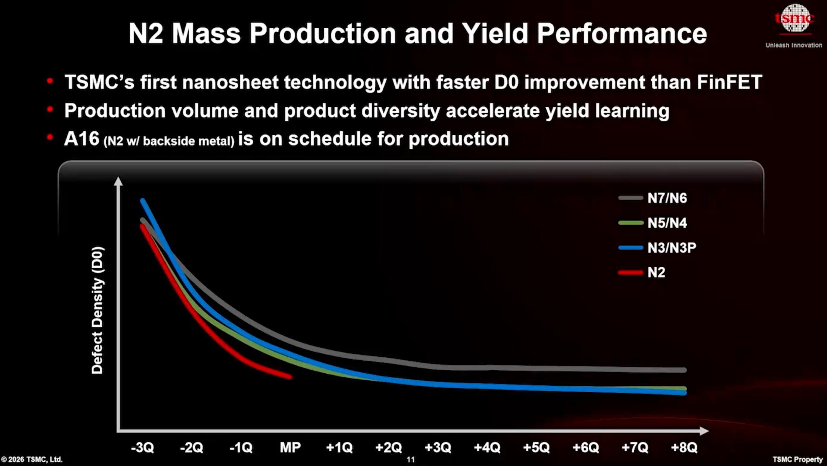
The central part of TSMC's expansion plan is its N2 process technology. At present, the company is ramping up production of chips using N2 at two sites: Fab 20 phase 1 and phase 2 in Hsinchu near TSMC's global R&D center, and Fab 22 phase 1 in Kaohsiung. Ramping a leading-edge node at three facilities simultaneously is highly uncommon for foundries. The company also plans to ramp up production at Fab 22 phase 2 shortly and Fab 22 phase 3 by the end of the year. Eventually, Fab 22 phase 4 will come online as well. As a result, TSMC aims to start mass production on its N2 process technology at five facilities in the first year, which is at an unprecedented scale.
(Image credit: TSMC)
(Image credit: TSMC)
(Image credit: TSMC)
(Image credit: TSMC)
As a result of such an aggressive ramp, TSMC expects its N2 wafer-out capacity to be 45% higher than that of N3B in the first year. Reports from 2023 – 2024 indicate that TSMC ramped its N3B production at two or three phases of Fab 18 in 2023 and reached a capacity of around 60,000 wafer starts per month by the end of that year. If the reports are accurate, then TSMC expects its N2 capacity to reach around 90,000 wafer starts per month (WSPM) by the end of the year. This exceeds the fully ramped capacity of Intel's 18A-capable Fab 52, which is believed to be at around 40,000 WSPM.
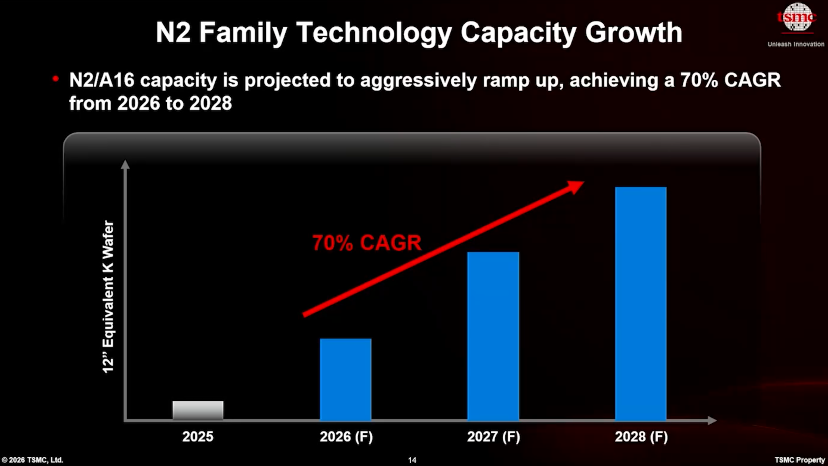
What is even more impressive is that TSMC intends to increase its N2/A16-capable capacity by 70% every year through 2028, which means hundreds of thousands of WSPM in 2029.
In addition to reaching vast capacity, ramping up five fab phases simultaneously enables TSMC to mitigate risks. If one fab phase experiences a contamination issue, tool failure, or yield issues, the entire N2 supply chain will not collapse. The same applies to ramping up production at two sites located in different parts of the country: an earthquake or utility failure can interrupt production or even cause yield loss at one of them, but it will not affect another. Such risk mitigation is critically important when customers like Apple, AMD, Nvidia, or Qualcomm, which demand a continuous supply. There is potentially another bonus with ramping up these fab phases in parallel rather than in serial, so read on.
N2 ramp: One Team and the Super Manufacturing Platform
Such an unusual ramp strategy seems to be enabled by two programs at TSMC: the "One Team" collaboration between R&D and fab operations, and the Super Manufacturing Platform (SMP) that enables multiple fabs (or rather fab phases) to work as one, which likely has similarities to Intel's "Copy Exactly". TSMC hasn't shared many details about the One Team and SMP, though we can make some educated guesses.
(Image credit: TSMC)
(Image credit: TSMC)
The One Team is a global manufacturing knowledge-transfer system that links R&D, process integration, equipment management, and high-volume manufacturing expertise during technology development and ramp. To speed up feedback loops, TSMC likely inserts manufacturing teams relatively early in node development so that R&D teams adjust their work to what is possible at fabs. As a result, yield learning, process optimization, and tool productivity improvements can be done quickly at one fab and then transferred to others. TSMC says that One Team enabled a 20% faster technology transfer compared to N3, without disclosing the time it typically takes to transfer technology from one fab to another.
In addition, all of TSMC's GigaFab sites now rely on its Super Manufacturing Platform (SMP), which is essentially a centralized manufacturing-control system that makes multiple fabs operate as one giant synchronized fab with standard process recipes, tool configurations, metrology, and yield management flows. This should enable TSMC to transfer production between fabs more easily, ramp new nodes faster, introduce yield fixes globally instead of locally, and reduce customer requalification work when production of chips is moved from one fab to another.
Moreover, since every fab phase generates its own tool behavior data, defect density data, process window statistics, and yield learning information, multiple simultaneous ramps may actually accelerate yield/defects learning when SMP and One Team are in place. In turn, it may speed up ramping of fab phases.
A 70% CAGR in N2/A16 capacity in the coming years is an extraordinarily aggressive ramp for leading-edge manufacturing. Without something like TSMC's' One Team structure and SMP, coordinating that scale of expansion across multiple Fab 22 phases, Fab 20, and eventually Fab 21 phase 3 in Arizona would be barely possible both from organizational (operational control) and from economic (yield learning, process window, etc.) points of view.
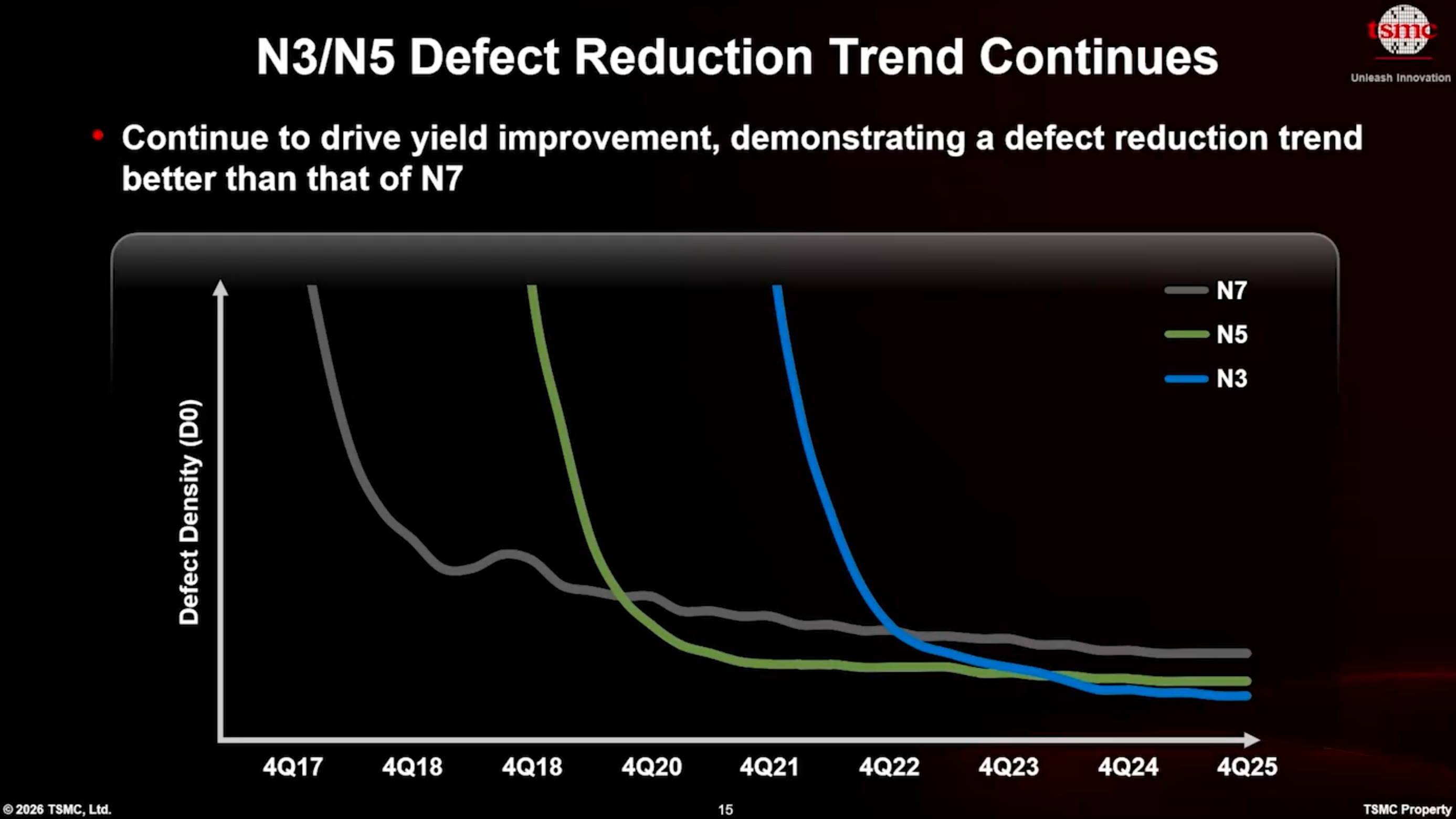
TSMC also noted that despite the significantly higher complexity associated with gate-all-around (GAA) nanosheet transistors, N2 is achieving a better yield learning curve than N3, which again can be attributed to the innovative approaches that the company uses.
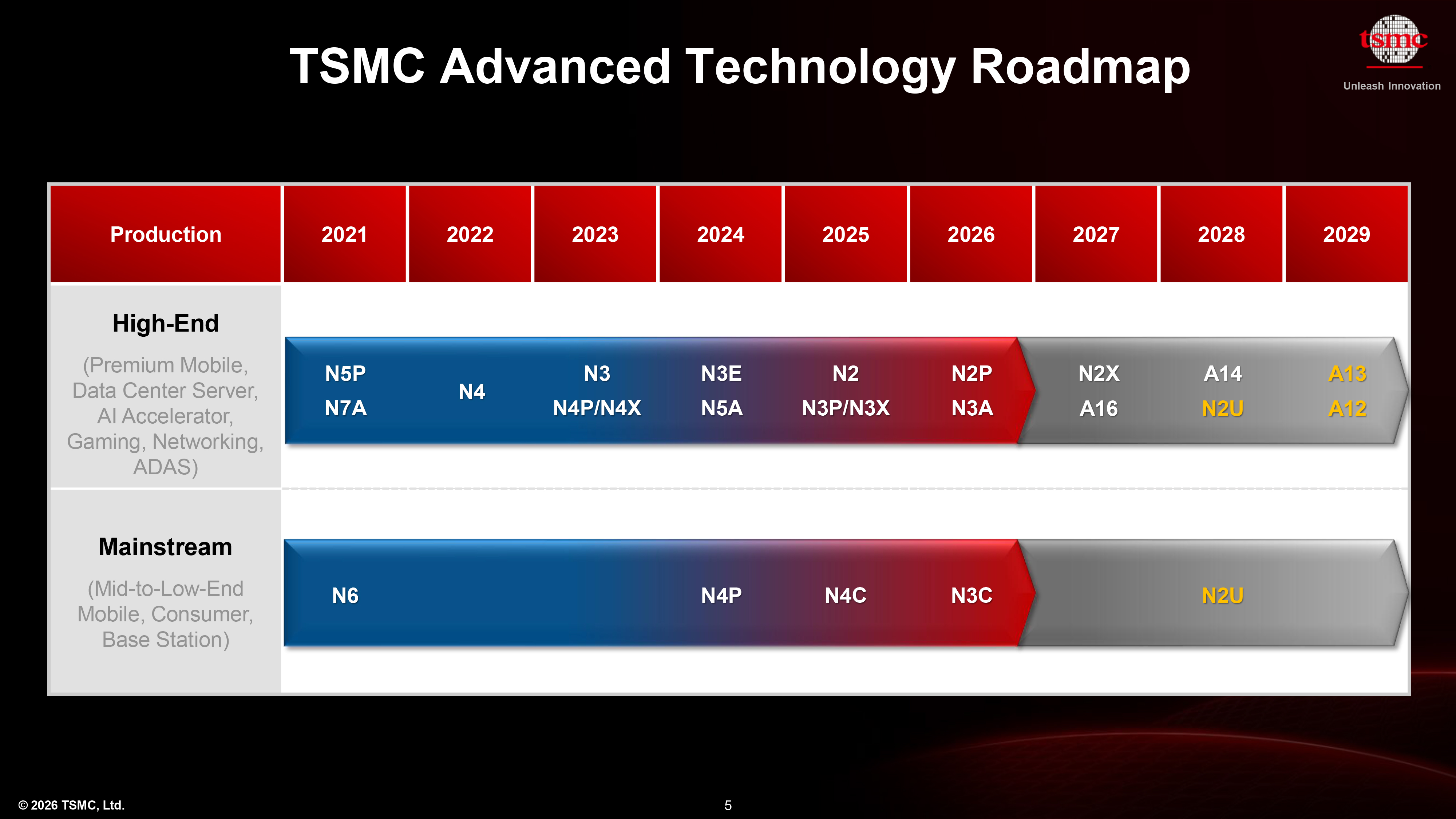
Beyond N2: A14, A13, and A12
TSMC's N2/N2P/N2X/N2U/A16 production will largely be concentrated at Fab 20 phase 1 and 2, Fab 22 phases 1, 2, 3, 4, and, to some degree, Fab 21 phase 3. However, for nodes beyond 2nm-class (A16 is essentially N2P with a backside power delivery network), such as A14, A13, and A12, TSMC will build Fab 21 phase 3 and then the all-new Fab 25 site in central Taiwan with at least four phases.
(Image credit: TSMC)
A14 is set to start high-volume production in late 2028, so there is a good chance that TSMC will ramp it at both Fab 20 phase 3 and Fab 25 phase 1. However, given the company's aggressive approach to capacity expansion, TSMC might well surprise us once again. Also, we do not yet know how TSMC plans to upgrade N2/A16-capable fabs to subsequent nodes, if at all.
Expansion beyond N2
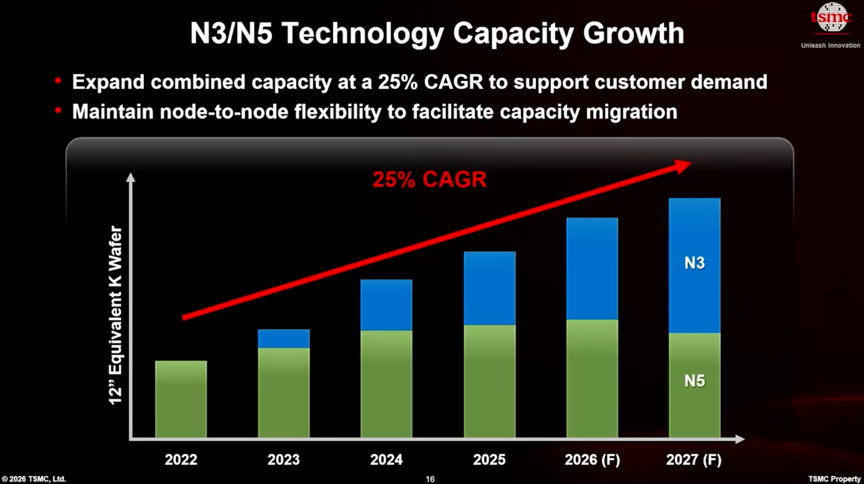
The expansion is not limited to the N2 production node and subsequent technologies. TSMC is continuing to grow combined N3 and N5 capacity at a 25% compound annual growth rate (CAGR) from 2022 through 2027. To address immediate demand, the company is converting some N5 capacity into N3 production, which is not particularly expensive, since N3 reuses 85% - 90% of the tools used for N5. Furthermore, as much of TSMC's N3 and N5 capacities are concentrated at Fab 18 (four phases N5, four phases N3), converting some of the N5 capacity to N3 is relatively easy from a logistical perspective.
(Image credit: TSMC)
(Image credit: TSMC)
AI is here to help (to build more AI processors)
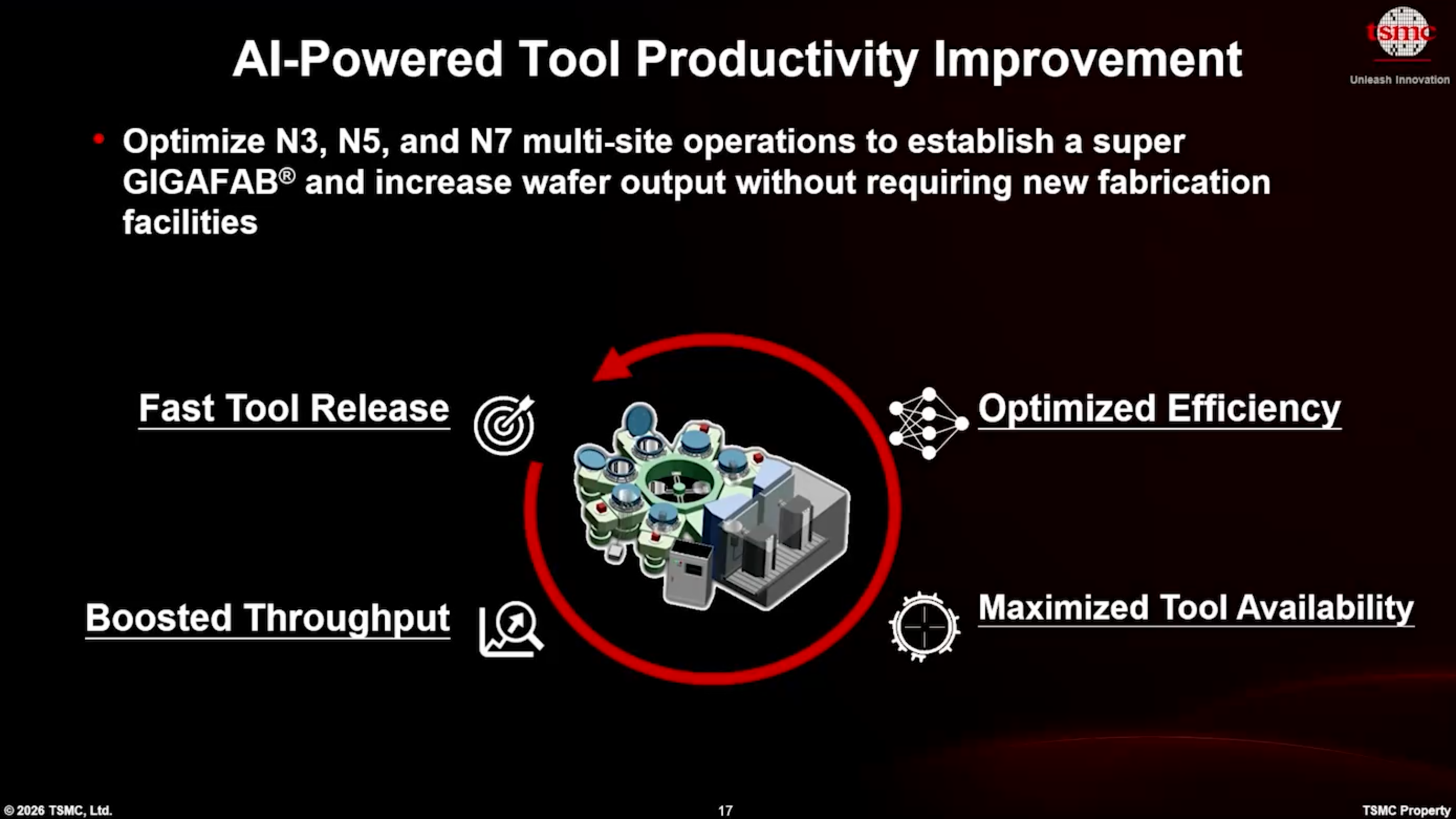
Alongside the conversion of N5 to N3 capacity, TSMC also heavily uses AI to improve the performance of each tool, and the whole fab in particular. Essentially, TSMC uses AI to build more AI processors, which seems to be a paradox, but it is becoming popularized as AI becomes embedded within workflows.
(Image credit: TSMC)
(Image credit: TSMC)
One of the things that greatly slows down cycle times of modern fabs is batch processing of wafers in various chambers, something that is an inevitable part of some 5,000 steps. Essentially, 25 wafers ‘wait’ in a (perhaps in a CVD chamber) for a lithography tool to process them individually.
Atsuyoshi Koike of Rapidus thinks differently and believes that a single-wafer processing across all steps can significantly speed up cycle time, but at the cost of tool efficiency. TSMC does not seem to plan to use single-wafer processing (despite its purchasing power, it can likely persuade fab tool makers to produce appropriate tools), but it can certainly optimize the ways how it uses existing tools to boost productivity of its existing fabs.
TSMC revealed at its recent Technology Summit that it uses intelligent scheduling systems that incorporate 'state-of-the-art linear programming and heuristic algorithms' to optimize equipment efficiency, though it did not reveal what exactly is done and what is achieved. TSMC further revealed that it uses generative AI algorithms to identify optimal parameters that 'challenge the physical limits of equipment' while maintaining wafer quality. In parallel, the company analyzes tool logs using big-data analytics and text-mining systems to dynamically adjust key parameters, minimize tool idle time, and maximize output.
AI systems are also used for real-time chamber condition analysis to determine optimal chamber-cleaning timing and avoid unnecessary maintenance that could reduce machine uptime and available capacity. In addition, TSMC disclosed that AI-assisted comparison and fine-tuning of large volumes of machine verification parameters reduced the time required to validate new tools and reach high-volume manufacturing by more than 20%, which helps to ramp up new fab modules faster.
TSMC also said it achieved more flexible allocation and higher combined N3 and N5 capacity at Fab 18 in Tainan by increasing equipment commonality and integrating 'cross-technologies planning,' which essentially means that the company re-uses as many tools as possible.
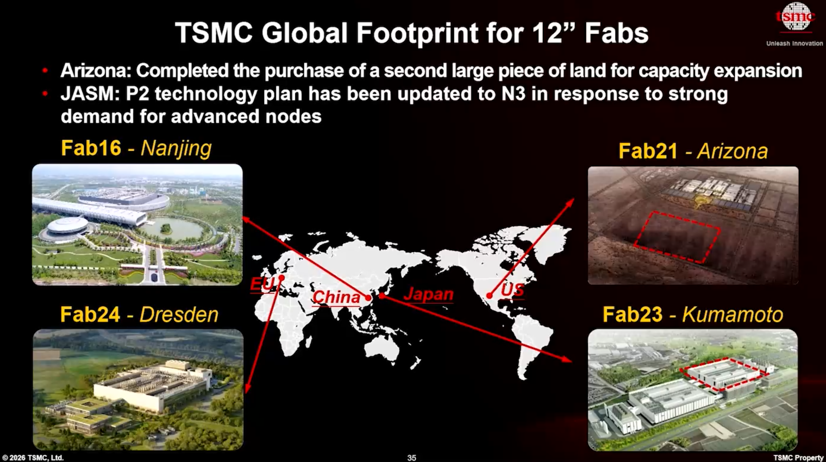
Expansion beyond Taiwan
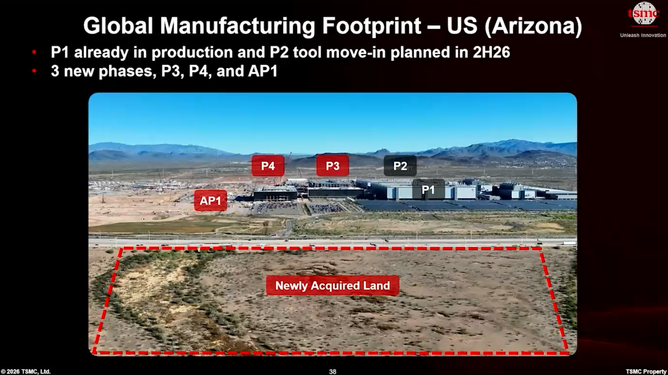
Outside of Taiwan, TSMC continues to broaden its geographic footprint. In Arizona, Fab 21 phase 1 is already producing chips using N4 technology (with capacity increasing by 1.8X this year alone), while Fab 21 phase 2 is on track to start N3 production in Q3 2027. Fab 21 phase 3 targets N2 sometime later this decade, as the company continues to construct shells both for phase 3 and phase 4. The company also reaffirmed plans for an advanced packaging facility, an R&D center, and additional land acquisitions to support future expansion.
(Image credit: TSMC)
(Image credit: TSMC)
(Image credit: TSMC)
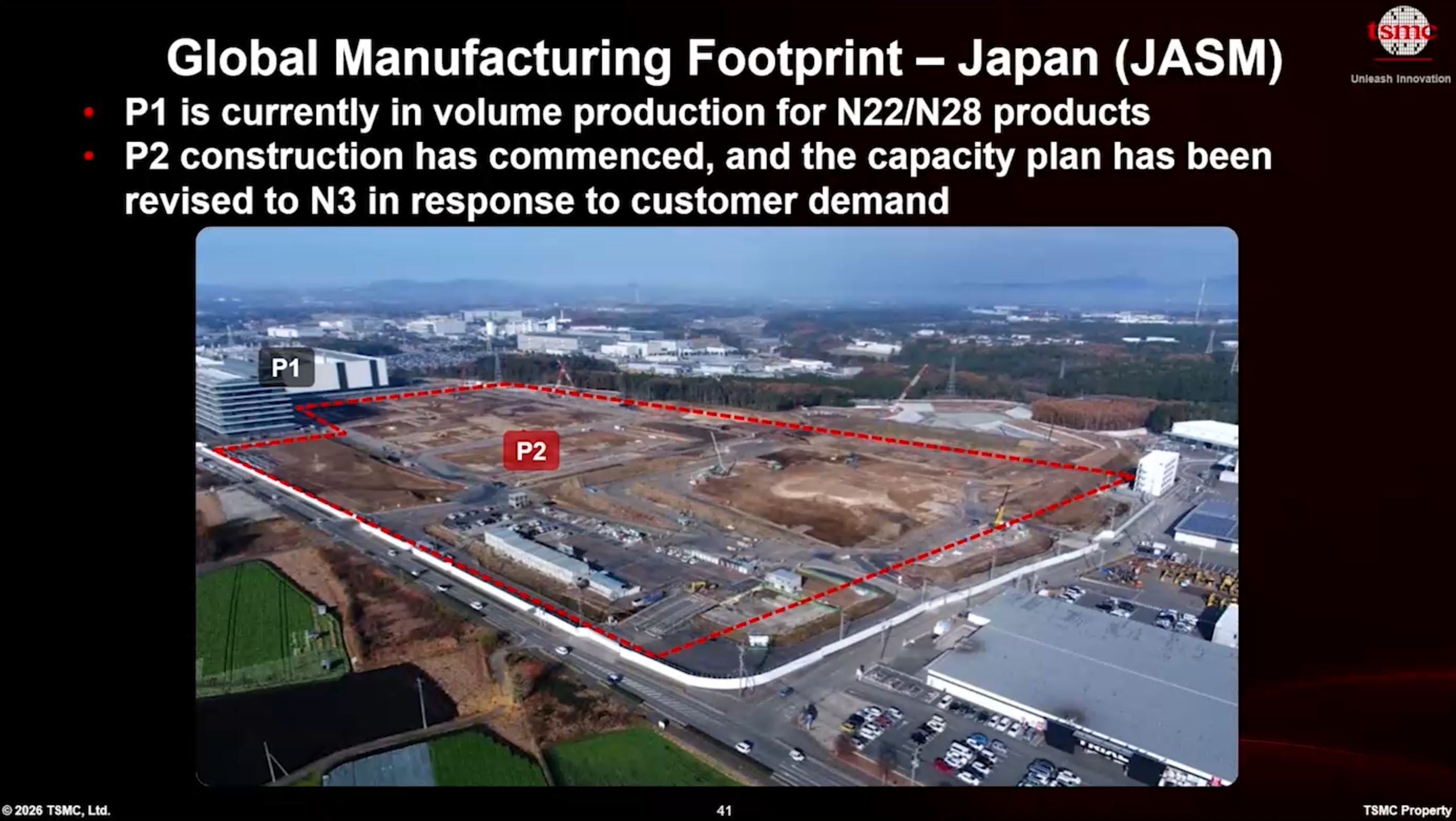
In Japan, the company’s Kumamoto Fab 23 phase 1 is already producing 28nm and 22nm chips, while Fab 23 phase 2 underwent a major strategic shift. Originally planned for 7nm-class production, the facility will instead manufacture using technologies down to N3 3nm to address stronger-than-expected local demand and onshoring intentions of local chip designers.
Meanwhile, Fab 23 in Dresden, Germany, which is under construction, is aimed at automotive and industrial applications with legacy planar transistors and FinFET-based 28nm, 22nm, N16, and N12 production nodes.
Advanced Packaging
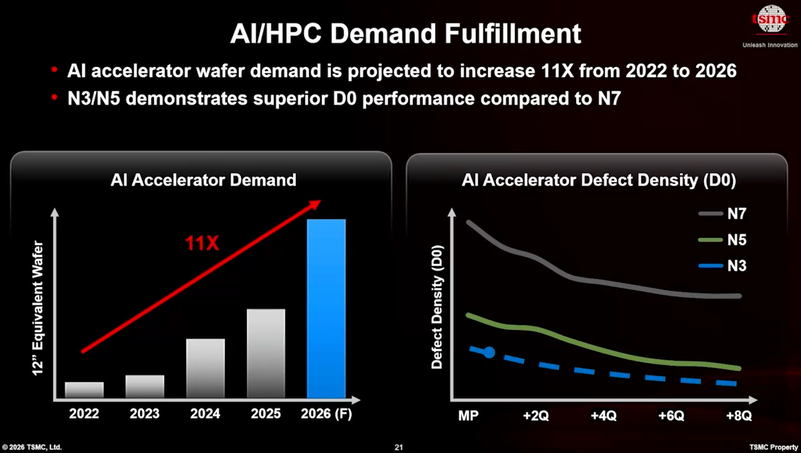
AI itself is now one of the main drivers behind the company's unprecedented capacity growth. TSMC disclosed that wafer shipments for AI accelerators are expected to rise 11X between 2022 and 2026. The company also highlighted the rapid growth of extremely large dies exceeding 500 mm2, as shipments of those devices are projected to increase 6X over the same period. Such products typically require lots of wafer capacity (wafer starts) and advanced packaging technologies, since many of these designs use HBM3E memory.
(Image credit: TSMC)
(Image credit: TSMC)
(Image credit: TSMC)
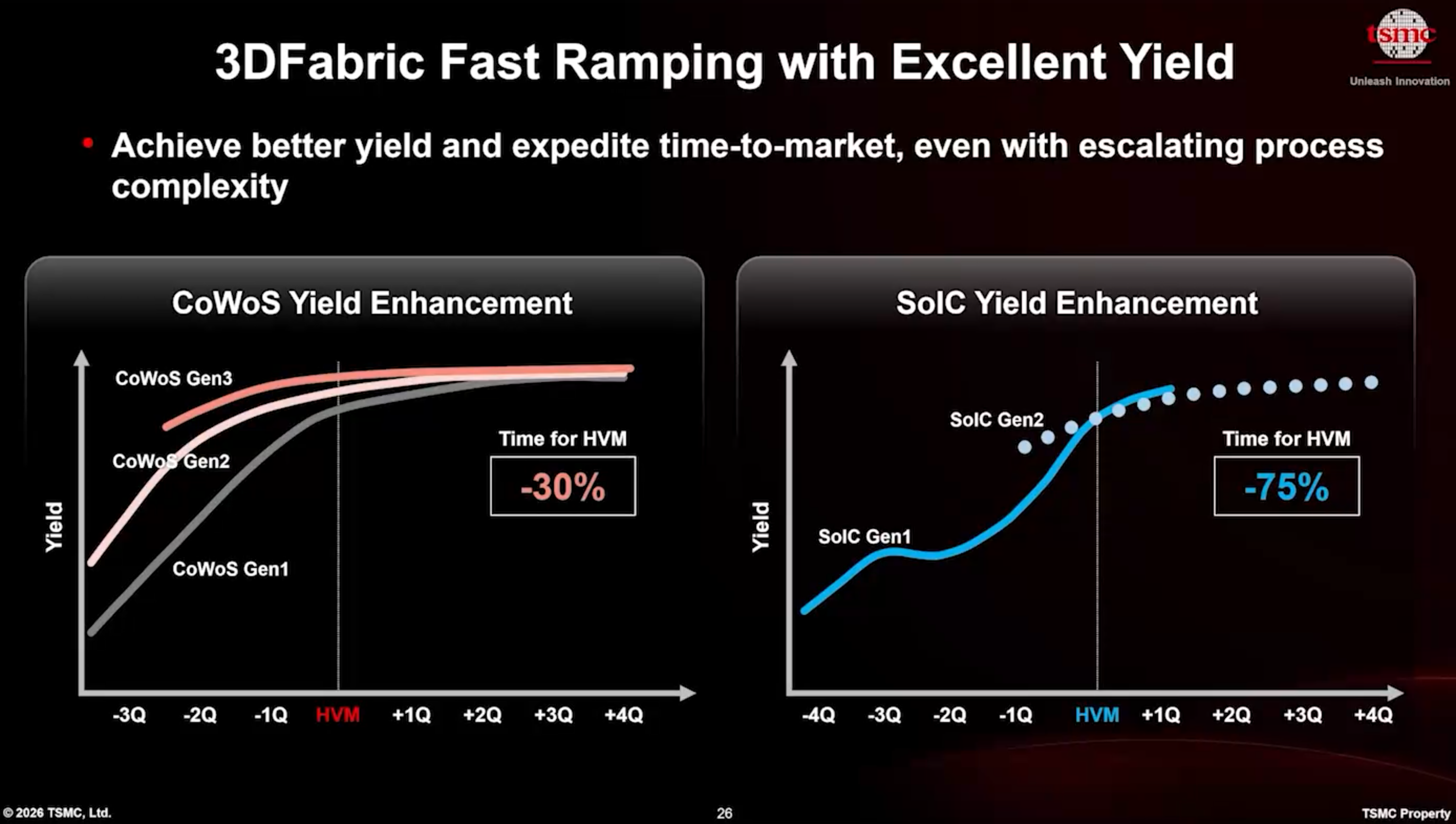
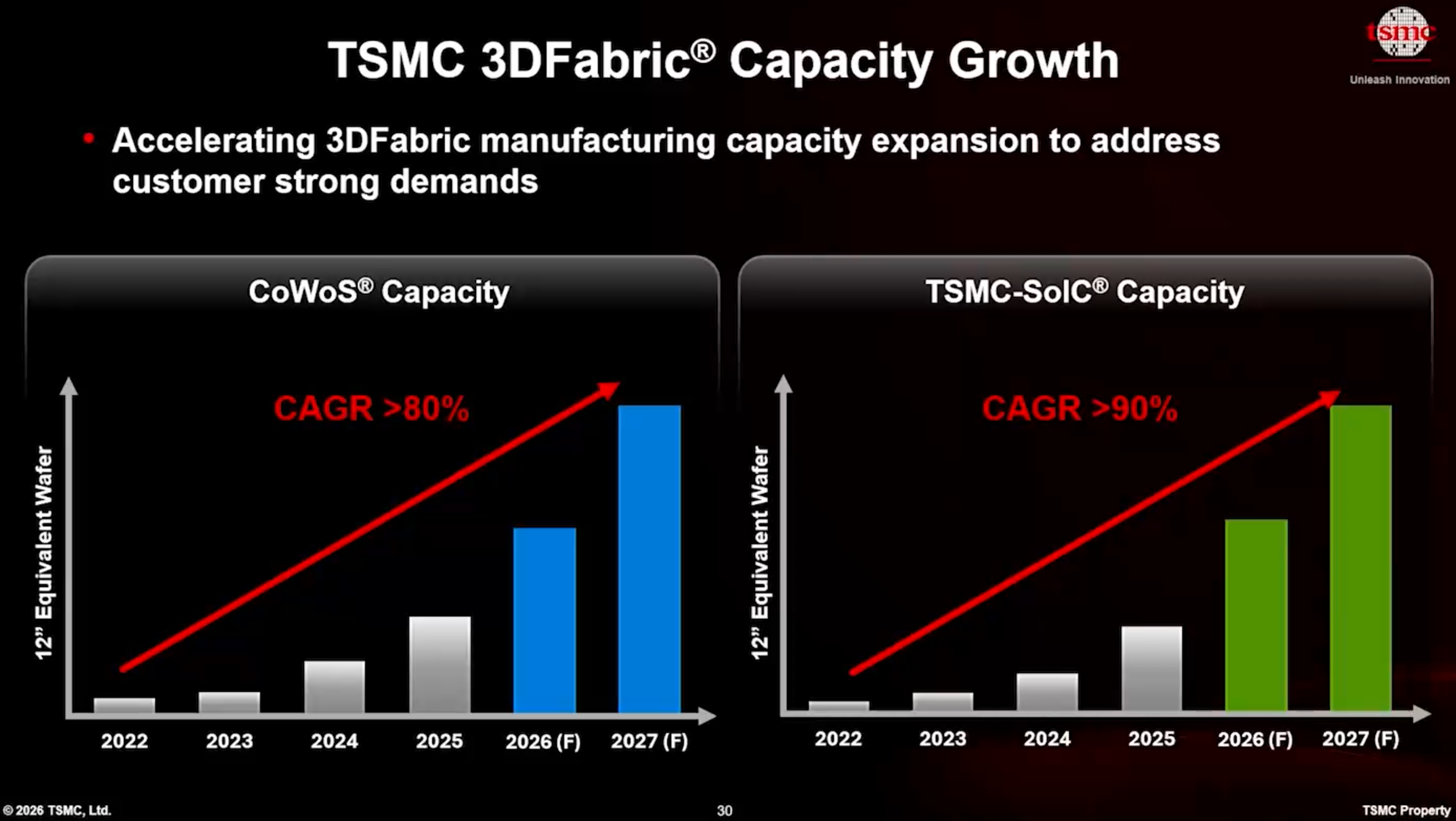
Advanced packaging has therefore become just as important as wafer fabrication itself. TSMC said its CoWoS capacity will grow at an 80% CAGR between 2022 and 2027, while SoIC capacity will expand at a 90% CAGR during the same timeframe. TSMC also said it has improved development-to-HVM transition times by 30% for CoWoS and by 75% for SoIC compared to earlier generations.
TSMC currently operates 11 advanced packaging facilities in Taiwan (AP1 in Hsinchu, AP2A/AP2B/AP2C and AP8 in Tainan, AP3 in Longtan, AP5 in Taichung, AP6A/AP6B/AP6C in Zhunan, and AP7 in Chiayi). According to a recentDigiTimes report, the company is simultaneously expanding multiple advanced packaging campuses, including AP5, AP6, AP7, and AP8.
The AP7 site in Chiayi will reportedly become TSMC's largest advanced packaging campus using SoIC to support major customers like Nvidia, which plans to use 3D packaging technologies for its next-generation Feynman GPUs. AP8 — converted from a former Innolux LCD fab — is expected to exceed 40,000 wafers per month of CoWoS capacity by late 2026.
While CoWoS is the de-facto standard for AI processors, SoIC is set to become much more widely used in the coming years. As a result, the company is also rapidly expanding its SoIC production capacity. DigiTimes claims that AP6 in Zhunan could approach 10,000 SoIC wafers per month, whereas AP7B may add approximately 12,000 wafers per month. Future AP7 phases are expected to support both SoIC and CoPoS technologies, though CoPoS is a part of TSMC's roadmap in the 2030s.
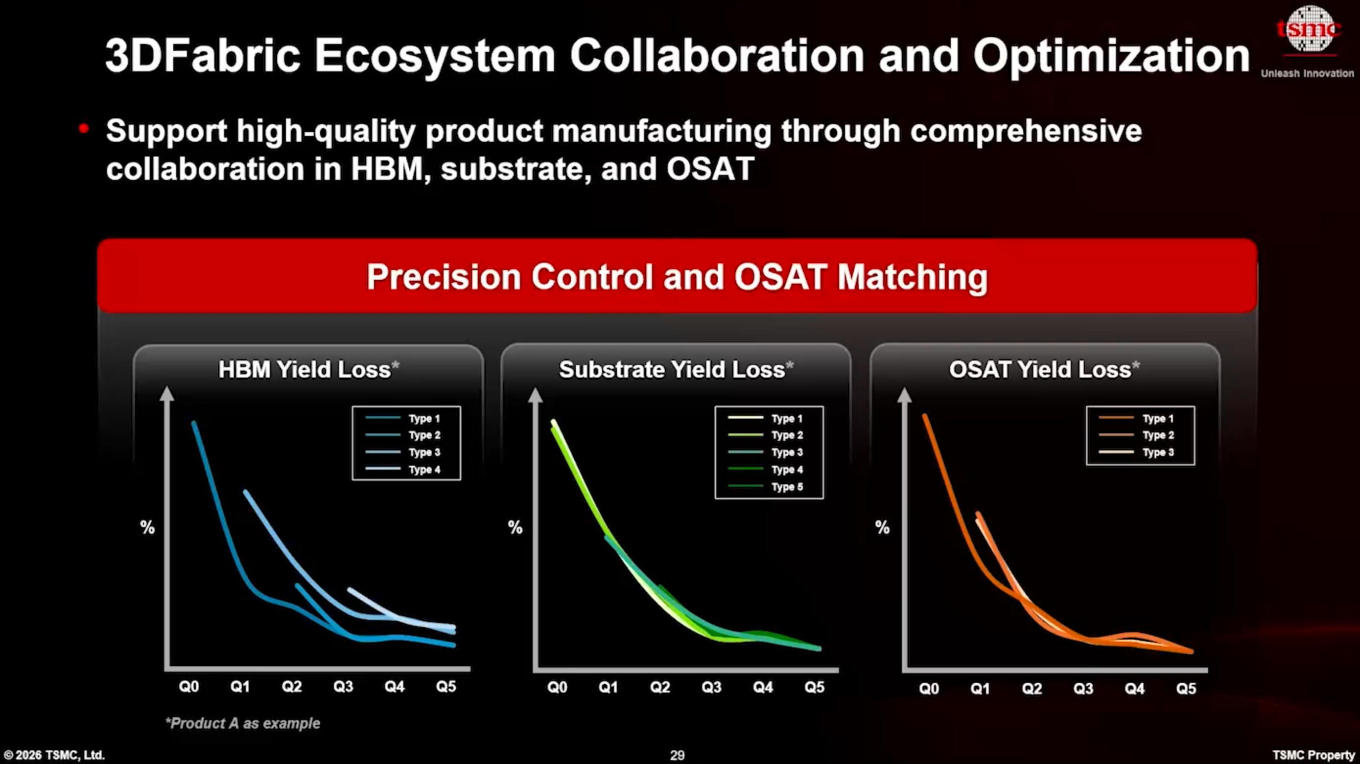
Advanced packaging now requires tight ecosystem integration that includes HBM suppliers, substrate vendors, OSAT partners, testing companies, materials providers, and toolmakers, with which TSMC works to standardize those tools. The very emergence of such an ecosystem emphasizes the increasing role of TSMC in the burgeoning AI industry.
An all-encompassing roadmap
After investing nearly $240 billion into capacity expansion over the last decade, TSMC has evolved from the world’s largest foundry into the world's largest producer of advanced logic chips, producing the lion's share of AI processors today.
(Image credit: TSMC)
To support the explosive AI demand and to stay ahead of Intel and Samsung Electronics, TSMC has doubled its historical fab construction pace to nine fab phases annually in 2025 – 2026 while simultaneously expanding in Taiwan, Arizona, Japan, and Germany. The company's N2 ramp is unprecedented as the company preps to ramp five fab phases within the node's first year, and N2/A16 capacity is projected to grow at a 70% CAGR through 2028.
TSMC said this aggressive expansion is enabled by its One Team organizational structure and Super Manufacturing Platform (SMP), which synchronizes manufacturing, yield learning, and process control across multiple fabs. The company is also implementing various AI-driven manufacturing optimizations, including intelligent scheduling systems, generative AI process tuning, and real-time tool analytics to improve throughput, reduce cycle times, and accelerate tool qualification.
At the same time, TSMC is rapidly expanding advanced packaging capacities. The company intends to increase CoWoS and SoIC capacities at 80% and 90% CAGR, respectively, through 2027, as demand for both technologies is expected to grow as chiplet-based designs and HBM memory are technologies of choice for AI accelerators.
*TSMC's wafer processing revenue for 2025 was $103,708.5 billion, thus representing around 84% of consolidated revenue of $122.4 billion. EUV-based N3 and N5 process technologies accounted for 60% of TSMC's wafer revenue in 2025, thus earning around $62,225 billion. Intel Foundry earned $17.826 billion in 2025, $307 million came from external customers that mainly ordered advanced packaging. It is estimated that process technologies that use EUV account for more than 10% but less than 20% of Intel's wafer revenue.
Intel does not disclose a revenue split similar to TSMC's (wafer fabrication vs. packaging/testing vs. other) in its official filings, so its wafer processing revenue is hard to estimate, especially given the fact that some of its silicon is made at TSMC and is packaged internally. Nonetheless, even 20% of Intel Foundry's 2025 revenue is $3.565 billion, which is over 17 times less than TSMC earns on its EUV-based nodes.
Anton Shilov is a contributing writer at Tom’s Hardware. Over the past couple of decades, he has covered everything from CPUs and GPUs to supercomputers and from modern process technologies and latest fab tools to high-tech industry trends.

 (Image credit: Getty Images / Jimmy Beunardeau)
 Like
0
Like
0
 Dislike
0
Dislike
0
 Love
0
Love
0
 Funny
0
Funny
0
 Wow
0
Wow
0
 Sad
0
Sad
0
 Angry
0
Angry
0


Comments (0)