

‘I did not foresee at all the social-media application, nor its impact on society': Inventor of the CMOS-based image sensor on how a technology designed to take photos in space has changed the way we view the world
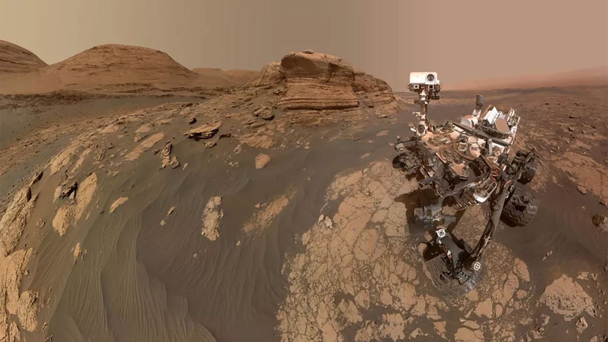
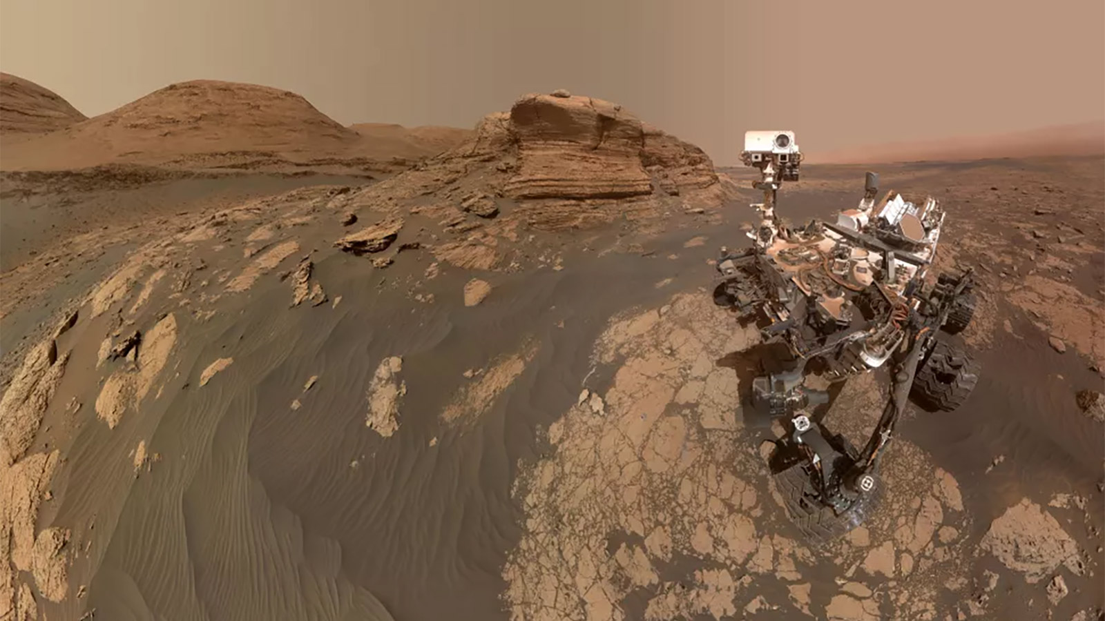 (Image credit: NASA/JPL-Caltech/MSSS)
Camera technology has come on leaps and bounds throughout the 20th and 21st century, but one of the most important developments was the invention of the CMOS image sensor. This invention, dubbed the ‘camera-on-a-chip’, is the technology that allows everyone to carry high-resolution cameras around in their pockets.
But the history of the CMOS can be traced back to NASA’s desire to install small, low-powered cameras capable of capturing high-resolution imagery on interplanetary spacecraft.
Dr. Eric R. Fossum is the inventor of the camera-on-a-chip, and he has not only fathered an era of space-based photography, but also the many industries and technologies that revolve around the micro-cameras we know today.
The camera-on-a-chip has changed the world
Before the development of the CMOS image sensor, photography and videography often relied on photographic film, or the more advanced Charge-Coupled Devices (CCDs). The Apollo 11 mission famously used purpose-built Hasselblad cameras - which were too heavy for the return trip to Earth - requiring the astronauts to transport just the film back for development. They’re still there to this day.
CCDs on the other hand were the precursor to Dr. Fossum’s camera-on-a-chip. They detected photons using individual pixels that fed an electrical charge to a single readout amplifier in a row-by-row configuration. These cameras improved significantly in reducing weight and capturing much more vivid imagery than their film-based counterparts, but suffered from high power-usage and heat generation.
CMOS image sensors improved further on the CCD design, giving each individual pixel its own local conversion circuit and amplifier allowing each pixel to be read simultaneously while significantly reducing the energy required per image taken and the heat generated by the camera.
CMOS image sensors are the basis upon which most modern cameras work - from the camera on your phone and in your doorbell, to the Advanced Driver Assistance Systems that power self-driving cars, and even the cameras still heading into space today.
Sign up to the TechRadar Pro newsletter to get all the top news, opinion, features and guidance your business needs to succeed!
I spoke to Dr. Fossum to understand how CMOS image sensors were developed and their impact on the world we know today.
- Eric, did you ever think that your invention - the CMOS-based image sensor - would have such an impact on society worldwide?
I thought it could become ubiquitous and thought it should become so, but my confidence that it would actually happen was low, due to all kinds of unknowns. I did not foresee at all the social-media application, nor its impact on society, nor its impact on citizen-newsgathering, nor its impact on social justice, whether to protect good actors in law enforcement or to identify bad actors in law enforcement. I also knew there could be impact on privacy and liberty, and I am uncomfortable with how that has evolved.
- I note that you worked at NASA's legendary JPL (Jet Propulsion Lab) at the time. We don't usually associate JPL with cutting-edge digital imaging. How did that happen? Was JPL essentially another Xerox PARC?
NASA and JPL is associated with cutting edge digital imaging, from its earliest activities in the robotic exploration of space. JPL engineers found ways to beam back images from distant places using digital imaging and data transmission. Eugene F. Lally at JPL in 1961 was probably the first advance the idea of a ‘mosaic’ image capture, where mosaic refers to an array of pixels. JPL developed many digital imaging technologies for scientific use in the harsh environment of space with high precision and reliable image capture across a larger range of wavelengths than consumer products. My job at JPL was created by JPL management to further grow JPL’s bench-depth in CCD technology.
- I am sure that you followed avidly the visual journey of Artemis II a few weeks ago: from the iconic photos to the videos that the crew and the entire team produced during that trip. Do you remember what your thoughts were when you first saw the wonderful pictures the crew delivered?
My initial thoughts focused on the impressive images, and I was pleased that humans have returned to the moon, at least into orbit for now. But it did occur to me that that it was also cool that NASA –invented image sensor technology, employed in a consumer smartphone (and digital camera), was used on the this NASA mission, further completing its promise to make cameras faster, cheaper and better.
- Your current research at Dartmouth centers heavily on the Quanta Image Sensor (QIS). Can you tell us more about what it is, how is it different from CMOS image sensors and why it is called Quanta (which I presume is the plural of Quantum).
In the CMOS QIS, due to its ultra-low readout noise, it is possible for the first time to discern individual photons via their generated photoelectrons, and to count with high accuracy the number of photoelectrons at each pixel, at room temperature, at low voltages, and without the use of avalanche gain. The CMOS QIS we developed at Dartmouth and later at the spin-off company Gigajot is, in essence, a CMOS image sensor that uses intra-pixel charge transfer (invented at JPL) and extremely low readout-node capacitance, to generate a large enough voltage signal from a single photoelectron to overcome background thermal noise in silicon.
The QIS concept, itself though, is technology agnostic, since it was about creating great images one photon at a time. Single-photon-avalanche photodiode (SPAD) technology has significantly advanced in the past 20+ years so that it is also becoming useful for image sensor implementation. A SPAD QIS has larger pixels and consumes much more power than the CMOS QIS, but offers time-tagging of pixel arrival far more accurate than CMOS QIS and is being produced as a foundry-process that is also easily integrated with CMOS circuits.
- How has the IEEE impacted your professional journey?
I have been a member of IEEE since I was a student and have since graduated to Life Fellow. Profession societies are very important for the dissemination of leading research among experts in the field, and IEEE is no exception. I have published many papers under the IEEE, in the sub-silos of Electron Devices and Solid-State Circuits, and have benefitted from IEEE meetings such as the International Electron Devices Meeting (IEDM) and International Solid-State Circuits Conference (ISSCC). IEEE was also a partner in the early days of what is now known at the International Image Sensor Workshop, that I and others founded in 1986.
- What is the future of consumer image sensors from your point of view given that mainstream smartphones regularly boasts sensors with hundreds of millions of pixels already and we've reached a plateau in terms of returns?
Certainly in the near term, image sensors and consumers have benefitted from 3D integration and stacked wafer devices. The on-chip integration of more advanced functions possibly including smart-image-sensor functions or edge offers new avenues for improving image capture and understanding right at the focal plane. This was something I dreamed of since the 1980’s when I was exploring, researching and writing about smart image sensors and focal-plane image processing, but it was too early in those days.
- What are your thoughts on PIS (Processing-in-sensor) which fuses compute, the image sensor and memory in one holistic system at the edge?
As mentioned, I have been thinking about this topic since I was a graduate student in the early 1980’s at Yale and then at Columbia University. I am not familiar with the acronym PIS (which might really be a poor choice!) but I do think it is very application dependent. Furthermore, there is a data communication and parallel processing problem where local pixel computing is easy, but global image computing, where different regions have to be analysed, is still difficult on the focal plane. This may result in avoiding the addition of extra power dissipation to the image sensor chip and instead partitioning the imaging system into two parts, local computing on the focal plane and regional or global computing off the focal plane.
- Today there are billions of cameras that capture the world in two dimensions, generating millions of Gigabytes worth of data. Have you ever been interested in exotic storage technologies (some of which use image sensors)?
I have not really worked much in exotic storage systems, although at Photobit, our spinoff from JPL, we worked with companies, from other startups to giants like AT&T Bell Labs, on readout of holographic optical memories. Although, at that time, we were just focused on the image sensor chip and high speed readout.
- Can you tell me about the significance of the IEEE Jun-Ichi Nishizawa Medal, and what this recognition means to you?
Gosh, who doesn’t like being recognised by your peers for your accomplishments? Still, it is a very humbling event and makes me reflect on the great people that I have had the chance to work with over the years. It has been such a privilege to work with these folks and take this journey together. As I always try to mention, the amazing CMOS image sensor technology we all use every day was made possible by the hard and innovative work of thousands of image sensor engineers around the globe.
- We're planning a special series towards the end of the year, looking at tools that thought leaders use in their everyday lives. Name one (either physical or software-based) that you consider to be critical to your daily work routine and why you chose it.
I think AI tools are great time-savers in finding and curating information, and I often learn much from their apparent knowledge, and sometimes from their insights. These days I use Co-Pilot a lot. But I am always concerned with whom, directly or indirectly, I am sharing information and ideas with. I think this is something we should all ponder and ask hard questions of the AI giants.

Follow TechRadar on Google News and add us as a preferred source to get our expert news, reviews, and opinion in your feeds.
Désiré has been musing and writing about technology during a career spanning four decades. He dabbled in website builders and web hosting when DHTML and frames were in vogue and started narrating about the impact of technology on society just before the start of the Y2K hysteria at the turn of the last millennium.
What's Your Reaction?
 Like
0
Like
0
 Dislike
0
Dislike
0
 Love
0
Love
0
 Funny
0
Funny
0
 Wow
0
Wow
0
 Sad
0
Sad
0
 Angry
0
Angry
0









Comments (0)