Intel's EMIB packaging gains traction as chip designers look to skirt TSMC's CoWoS constraints — Google's reported decision for 9th-gen TPUs highlights Intel's attractive alternative
Jul 15, 2026 - 19:09
03
(Image credit: Google)
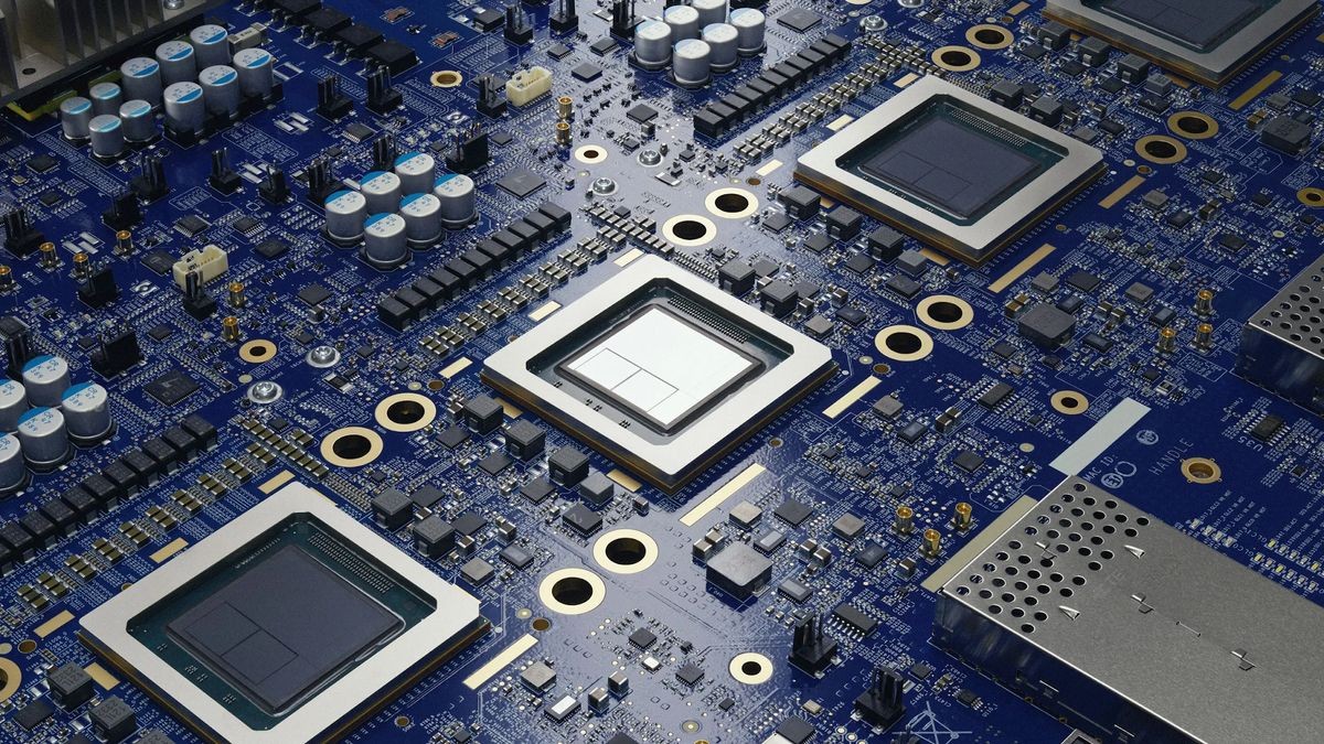
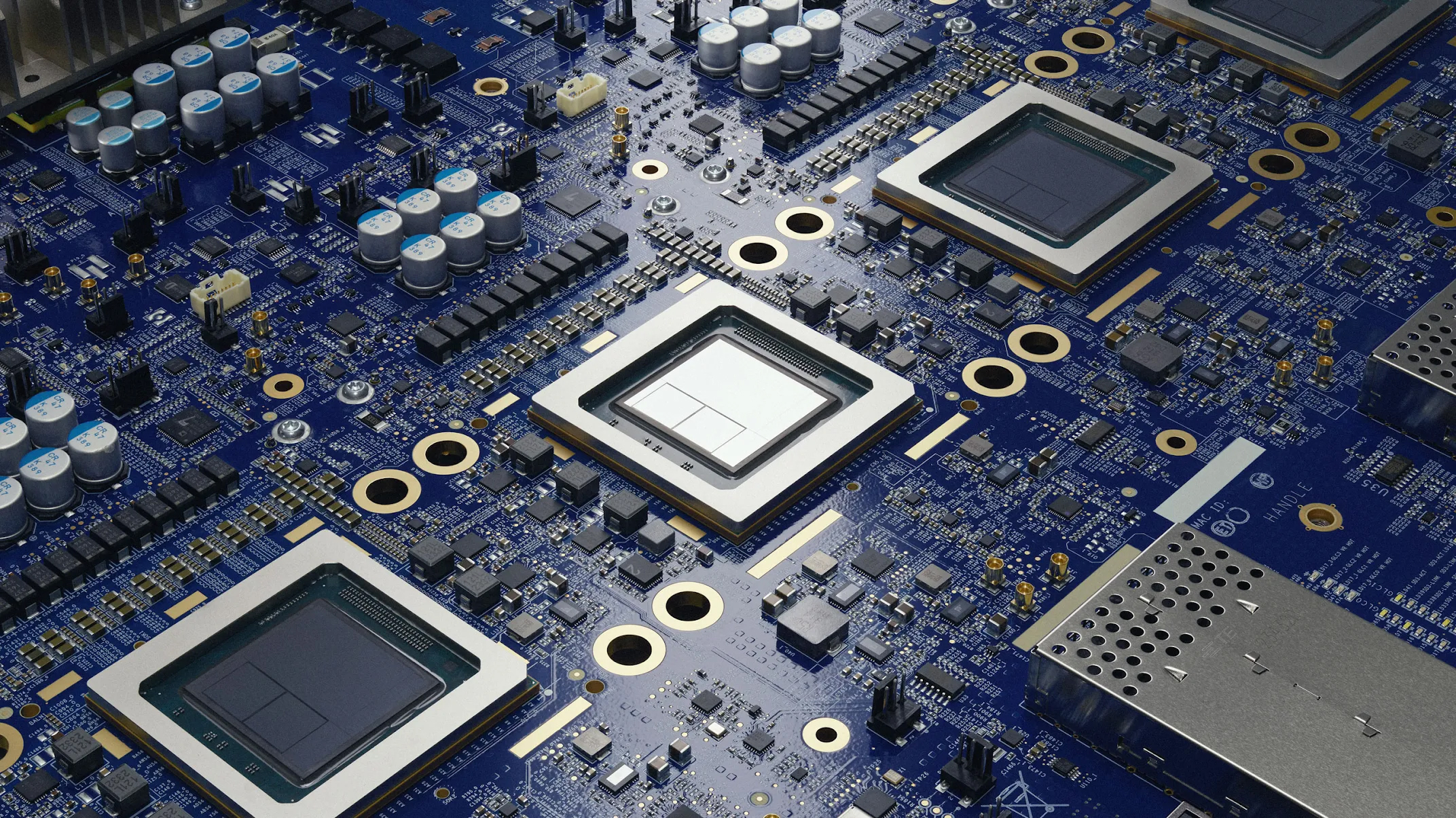
Google plans to use Intel's EMIB-T packaging for its next-generation TPU codenamed Humufish, according to SemiAnalysis. TSMC's portfolio of chip-on-wafer-on-substrate (CoWoS) technologies has become the de facto standard advanced packaging option for nearly all AI and HPC processors made in the industry. Competing offerings are usually considered as secondary solutions if CoWoS is in tight supply, but things are beginning to change.
Google is a long-standing CoWoS customer for TPUs, starting from the Third-Generation TPU, all the way to Google's latest Eighth-Generation TPUs. Assuming that SemiAnalysis's report about Google's decision to move to EMIB-T with its Ninth-Generation TPUs is accurate, it's a big decision for Google, as switching from one advanced packaging technology to another is a complicated endeavor, which involves plenty of changes and unknowns. Understanding Google's reasons for the switch could shed some light on the prospects of Intel's and TSMC's advanced packaging technologies, which will be used by leading chip designers and hyperscalers in the coming years.
Advanced packaging technologies at glance
For years, Google used TSMC's CoWoS-S, and later, CoWoS-L packaging. Initially, the company used CoWoS-S packaging, which relies on a silicon interposer up to 3.3X the reticle size, but with its 7th- and 8th-Generation TPUs, the company moved to CoWoS-L. CoWoS-L relies on a redistribution layer (RDL) interposer with embedded local silicon interconnect (LSI) bridges that enable high-performance die-to-die links, which can scale packages to 5.5X the reticle size today. TSMC promises to improve CoWoS-L's capabilities to scale over 14X the reticle size by the end of the decade.
(Image credit: Intel)
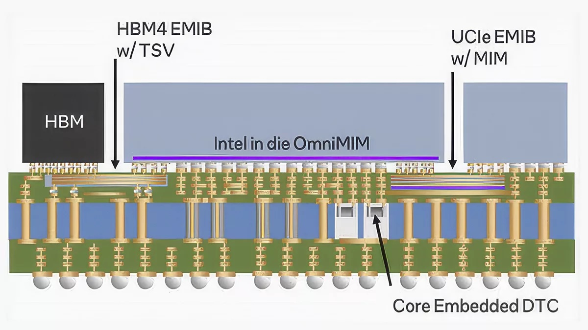
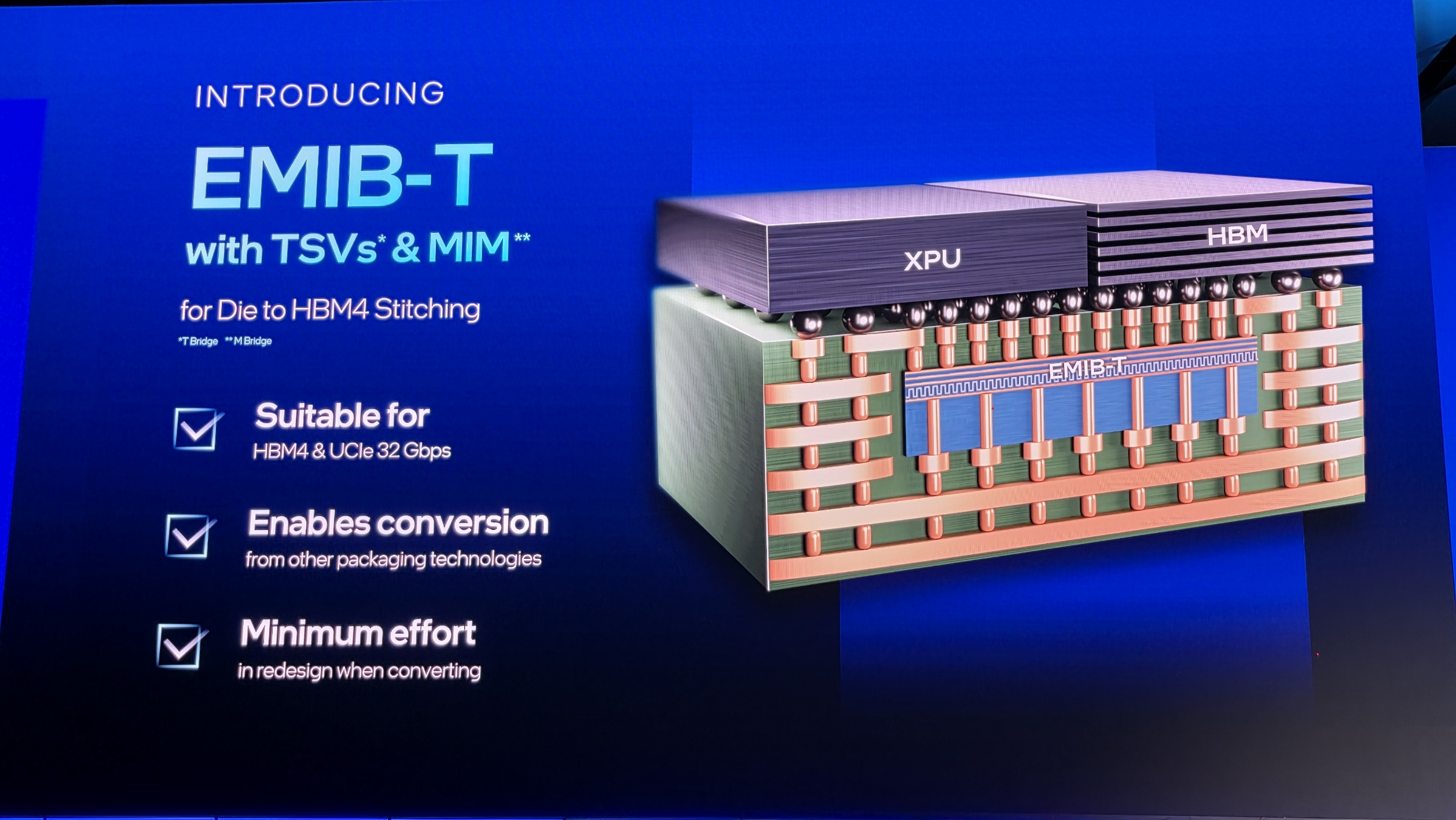
Unlike CoWoS, Intel's embedded multi-die interconnect bridge (EMIB) technology does not use any interposers. The technology instead relies on tiny embedded silicon bridges within the substrate to enable high-density die-to-die interconnections, whereas everything else is routed through an inexpensive organic substrate.
EMIB-T adds through-silicon vias (TSVs) to the bridge, which enables power to flow vertically instead of going through the organic substrate. In addition, Intel's EMIB-T also integrates sophisticated metal-insulator-metal (MIM) capacitors and a dedicated ground plane into the bridge to improve power integrity. The latter is a particularly important feature of complex next-generation AI accelerators, which demand more, cleaner power, and for which power delivery is becoming as challenging as signal routing.
The main selling point of EMIB (and EMIB-T) is that it is not constrained by interposer reticle limits as it places small silicon bridges only where high-density die-to-die links are needed. Strictly speaking, CoWoS-L is not either, as it uses LSIs locally as well. The difference is that those bridges are embedded into a package-wide RDL interposer that connects everything and enables dense interconnections across the package.
Since both CoWoS-L and EMIB-T are designed to address the same applications and have many similarities in the way they do this, the choice between them is likely driven by a combination of factors rather than one single advantage or disadvantage. On the technology side of matters, these factors include interconnect performance and density, power delivery, scaling beyond very large package sizes, and mechanical rigidity. On the business side of things, costs, capacity availability, and supply chain diversification are also a significant factor.
Crucial differences
(Image credit: Tom's Hardware)
SemiAnalysis claims that the main advantage of EMIB/EMIB-T over CoWoS is the lack of reticle limit, but this argument does not fully hold against CoWoS-L, as it was invented specifically to escape the reticle limitation by replacing the monolithic silicon interposer with localized LSI bridges.
When it comes to dense, package-wide routing, CoWoS-L's RDL interposer is fundamentally superior to an ordinary organic substrate offered by EMIB-T. Organic substrate wiring has coarser line/space dimensions and larger vias, so it cannot provide the same routing density as CoWoS-L's fine-pitch RDL. Where an EMIB bridge connects adjacent dies, Intel can achieve very high interconnect density. But anything that needs to travel beyond those bridges must use the package substrate or cross a topology involving additional bridges.
By contrast, CoWoS-L gives the designer two levels of connectivity: LSIs provide extremely dense local die-to-die connections, while the global RDL interposer provides relatively dense and flexible routing across the entire package. This means the RDL can carry longer, lower-density connections without consuming valuable LSI resources, while still offering much finer routing than the underlying package substrate.
One scenario for Google's choice is that it potentially wanted better power deliverythan what CoWoS-L could offer. EMIB-T integrates TSVs for vertical power delivery, sophisticated MIM capacitors for local decoupling, and a dedicated ground plane into its silicon bridges. The combination of these features substantially reduces power-delivery impedance and improves transient response and power integrity, which gives EMIB-T a major advantage over conventional EMIB for power-hungry AI accelerators. However, we have no idea how EMIB-T stacks up against CoWoS-L in the case of Google’s Humufish.
Of course, the larger the RDL interposer becomes, the greater its parasitics can become, potentially limiting scaling unless TSMC finds ways to mitigate them. However, EMIB does not eliminate long-distance wiring: If two distant dies must communicate, those signals still have to travel somewhere, and routing them through an organic substrate is not inherently electrically superior to routing them through a purpose-built RDL interposer. Therefore, it is difficult to claim that Google chose EMIB-T over CoWoS-L, simply because EMIB-T offers superior package-wide electrical characteristics.
After Nvidia suffered yield loss with its Blackwell data center GPUs due to an alleged mismatch in the coefficient of thermal expansion (CTE) among the GPU chiplets, LSI bridges, RDL interposer, and motherboard substrate, which led to warping and system failure, it is reasonable to question the mechanical rigidity of CoWoS-L packages. Nvidia has found a solution for its dual compute chiplet Blackwell packages, and so have other developers of AI accelerators. However, as package dimensions increase, they may behave differently, therefore causing yield losses.
By contrast, EMIB/EMIB-T eliminates the large RDL interposer and embeds small silicon bridges in the organic substrate, so most of the package consists of the substrate itself. This does not make EMIB/EMIB-T packages immune to mechanical failures, as large packages can warp and bend, causing various problems. However, as such packages lack the very source of global thermomechanical stress, they can potentially be more robust mechanically. However, EMIB-T can potentially complicate things because TSVs, additional metal structures, MIM capacitors, and their ground plane make the bridge more complex. Thus, Intel must manage both global package warpage and local stresses around each embedded bridge to ensure the mechanical rigidity of these packages.
Ironically, while CoWoS-L can offer denser package-wide routing, which is better for ultra-large processors, EMIB-T may potentially provide better mechanical rigidity required for such devices. Nonetheless, EMIB-T and its organic substrate do not eliminate package bending or cracking risks entirely.
Economics
If Google's Humufish TPU really moves to EMIB-T, the decision could well be both technical and strategic. Google has the engineering resources to opt for an all-new packaging technology in an effort to lower costs and eliminate dependence on TSMC's constrained CoWoS capacity. Nvidia tends to procure advanced packaging allocations years in advance, so it is possible that Google could simply not get enough CoWoS-L wafers for its 9th-generation TPU.
As a bonus, Google can also build relationships with Intel Foundry without using the company's fabrication technologies. In fact, keeping in mind that Intel and Google already have a strategic agreement covering Intel Xeon CPUs, it wouldn't be too surprising to learn that the cloud giant is courting Intel Foundry as well.
Both Intel's EMIB-T and TSMC's CoWoS-L have their own technological and economic advantages and disadvantages. Perhaps the biggest advantage of CoWoS-L is its predictability, as the company has experience with that tech. However, if Google has decided to drop that predictability in favor of an all-new packaging method, it may well have a combination of technological and strategic reasons to do so.
Anton Shilov is a contributing writer at Tom’s Hardware. Over the past couple of decades, he has covered everything from CPUs and GPUs to supercomputers and from modern process technologies and latest fab tools to high-tech industry trends.
 (Image credit: Google)
 Like
0
Like
0
 Dislike
0
Dislike
0
 Love
0
Love
0
 Funny
0
Funny
0
 Wow
0
Wow
0
 Sad
0
Sad
0
 Angry
0
Angry
0








Comments (0)