GlobalFoundries unveils 7nm-class FDX Fusion node — comes 7 years after firm abandoned FinFET
Oct 12, 2026 - 19:10
02
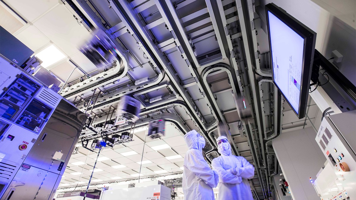
(Image credit: GlobalFoundries)
When GlobalFoundries abandoned development of leading-edge nodes in 2018, it also canceled the development of its 7nm-class FinFET fabrication technology that it co-developed with IBM. Almost exactly eight years later, GlobalFoundries is back with a 7nm-class manufacturing process, only this time the node relies on planar transistors and fully-depleted silicon-on-insulator (FD-SOI). It is aimed at automotive, edge AI, industrial, robotics, sensors, and other devices that prioritize low power consumption, high integration, and cost efficiency over maximum performance.
"We are delighted that GlobalFoundries has announced its next-generation 'single-digit FD-SOI; node, building on technology that CEA-Leti has been advancing for decades," said Sébastien Dauvé, chief executive of CEA Leti. "Through the FAMES pilot line, CEA-Leti continues to shape the future European roadmap for FD-SOI and works every day to promote its adoption in a wide range of applications."
FDX Fusion enters the scene
The new fabrication technology from GlobalFoundries is called FDX Fusion, and it promises 7nm-class 'digital performance' (an ambiguous claim; we will try to interpret it later) and more than twice the transistor density of its original 22FDX process introduced circa 2015. To achieve its target goals, the first generation of FDX Fusion will combine innovations in SOI substrates, transistor structures, and back-end interconnects, though keep in mind that GF has not disclosed transistor dimensions, contacted gate pitch, minimum metal pitch, or actual transistor density. GF plans to launch production of chips on FDX Fusion at its Dresden, Germany, facility in 2028, which will mark its return to the development of substantially more advanced FD-SOI fabrication processes after years of efforts to enhance its existing 22nm-class platform.
In addition to improved 'digital performance,' FDX Fusion will support RF transistors with fT/fmax of up to 0.5 THz, analog and mixed-signal circuitry, embedded nonvolatile memory, and in-memory computing capabilities. The combination is intended to enable highly integrated chips that can process information from sensors, execute AI inference workloads, control external devices, and communicate wirelessly without the need for numerous separate ICs. GF also intends to provide processor IP based on MIPS, ARC, and RISC-V architectures to accelerate the development of such products.
That being said, the main selling point of FDX Fusion is not necessarily its 7nm-class 'digital performance' and high-performance processor IP, but rather its ability to combine relatively powerful digital logic with RF, analog and mixed-signal circuitry, embedded nonvolatile memory, and in-memory computing capabilities on a single chip. This combination — which is why GloFo calls the process technology FDX Fusion — could enable highly integrated SoCs that would otherwise require multiple chips manufactured on different process technologies, which means additional tapeout costs as well as power consumption.
GlobalFoundries said it plans to deliver initial demo silicon for customer evaluation in early 2027, followed by the first process design kit (PDK) in mid-2027. The company is already collaborating with several customers on the technology, although it has not identified specific products or committed production volumes. Specifically, GF mentioned in its press release that BMW, Bosch, Infineon, NXP, Siemens, and Tesla have expressed interest in FDX Fusion, though only Infineon specifically confirmed collaboration on future 7nm-class technologies for radar and wireless communications.
Significant development
The GlobalFoundries announcement represents a significant development for GF's FD-SOI roadmap. The company introduced 22FDX in 2015 and announced its 12FDX successor in 2016, which promised performance comparable to 10nm FinFET, full-node density improvements, and up to 50% lower power consumption. Initial 12FDX customer tape-outs were expected in 2019, but the technology has never been adopted for commercial products. Instead, GF focused on enhancements to 22FDX and eventually the introduction of 22FDX+ (around the time when Samsung unveiled its 18FDS+), with additional capabilities for RF, embedded memory, and low-power applications. Interestingly, 12FDX was still a part of GF's investor roadmap in 2022.
FDX Fusion could therefore represent the realization of GF's original ambitions to scale FD-SOI beyond 22nm-class, although the company has not explained whether the new technology incorporates developments from its earlier 12FDX program. Meanwhile, CEA-Leti, which has conducted research into advanced FD-SOI technologies for years, describes FDX Fusion as a single-digit FD-SOI node. Nonetheless, GF's claim of 7nm-class 'digital performance' does not necessarily imply comparable transistor dimensions or integration density.
Get Tom's Hardware's best news and in-depth reviews, straight to your inbox.
From an industry perspective, FDX Fusion could provide an alternative to advanced FinFET and perhaps even gate-all-around processes for applications that require reasonably powerful digital logic alongside RF, analog, and embedded memory. Such integration could reduce system complexity and power consumption, particularly in edge AI devices where energy efficiency and real-time responsiveness are critical.
Perhaps more importantly, the technology could give European semiconductor developers access to a more advanced locally manufactured process without dependence on leading-edge foundries in Asia or the U.S.
Questions remain
However, the commercial success of FDX Fusion will depend on its actual performance, density, production costs, and the availability of a competitive design ecosystem, the latter arguably being the hardest part given the lack of any comments from leading electronic design automation (EDA) and IP developers.
When GlobalFoundries claims 2X 'digital performance' comparable to that of 7nm-class technologies, it doesn't reveal whether it means transistor switching speed, standard cell performance, achievable operating frequency, or something else. In addition, the company promises more than twice the logic density of its first-generation FDX technology, although the firm does not reveal any actual numbers. Consequently, it is unclear how FDX Fusion will compare with established 7nm-class FinFET technologies, which offer mature defect density and yields, plenty of supply, an established design ecosystem, and predictable pricing among other things, in terms of transistor density, performance, power consumption, and production costs. While CEA-Leti's comment seems promising, actual numbers are always better.
The very fact that GF's FDX Fusion planned 2028 introduction will come roughly nine years after the originally anticipated first 12FDX tape-outs illustrates significant technological and/or financial difficulties associated with the development of FD-SOI beyond the 22nm generation. So, while GlobalFoundries' FDX Fusion initiative certainly looks promising, it remains to be seen how that is going to play out for the contract chipmaker and its clients.
For now, the lineup of supporters from the automotive and industrial sectors — BMW, Bosch, Infineon, NXP, Siemens, and Tesla — certainly looks promising. But what about other applications? While established semiconductor companies such as Infineon and NXP already possess extensive processor IP portfolios, smaller fabless developers could benefit from GF’s MIPS and ARC processor cores, RISC-V expertise, and custom chip design capabilities, which could substantially reduce the cost and complexity of developing specialized SoCs. Still, to attract a broader range of chip developers, GlobalFoundries will need a mature ecosystem of EDA tools, standard-cell libraries, memory compilers, interface IP, and other silicon-proven building blocks. These are the things that GlobalFoundries has not touched upon in its press release.
Anton Shilov is a contributing writer at Tom’s Hardware. Over the past couple of decades, he has covered everything from CPUs and GPUs to supercomputers and from modern process technologies and latest fab tools to high-tech industry trends.


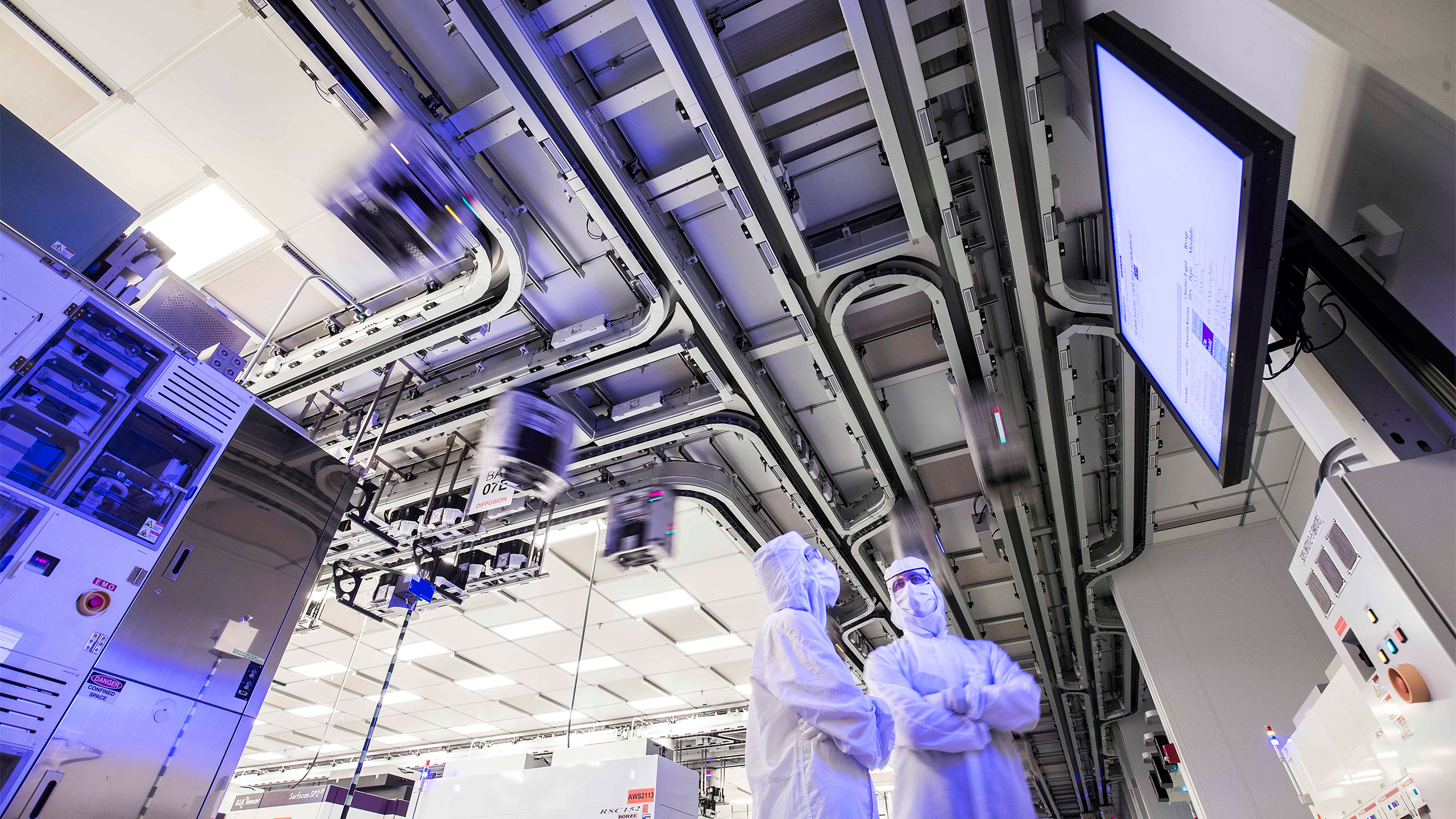 (Image credit: GlobalFoundries)

 Like
0
Like
0
 Dislike
0
Dislike
0
 Love
0
Love
0
 Funny
0
Funny
0
 Wow
0
Wow
0
 Sad
0
Sad
0
 Angry
0
Angry
0









Comments (0)