TSMC, Samsung, and Intel shore up support with ASML to deploy larger High-NA EUV photomasks — 6×12-inch photomask transition may take years despite unified effort
Sep 10, 2026 - 16:13
033
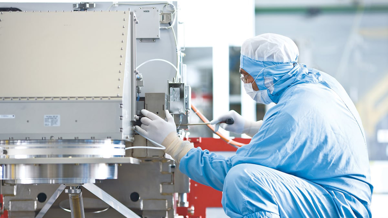
(Image credit: ASML)
ASML, Intel, Samsung, and TSMC are teaming up to drive the industry transition to 6×12-inch photomasks (reticles). This shift is paramount for High-NA EUV lithography, as the larger stencil would enable printing large chips in a single pass, instead of having to stitch smaller designs together, as ASML explained in a press release this week.
This kind of collaboration between chipmakers isn't entirely unheard of, but it is rare. But when they face an industry-wide challenge, they set aside their rivalry and join forces to move the industry forward. This happened several times in recent decades, first with the failed transition to 450-mm wafers co-funded by GlobalFoundries, IBM, Intel, Samsung, TSMC, and New York State, then with the EUV transition, which was spearheaded by Intel, TSMC, and Samsung.
Higher resolution comes with a nuance
High-NA EUV lithography is a major step forward from today's Low-NA EUV tools. With a numerical aperture of 0.55, High-NA systems can achieve an 8nm single-exposure resolution, compared with 13nm for 0.33-NA EUV scanners. The higher resolution enables chipmakers to pattern smaller, denser features in a single exposure, replacing complex Low-NA EUV multipatterning schemes with a single High-NA exposure. This can reduce the number of masks and process steps, shorten manufacturing cycle times, and potentially improve pattern fidelity and yields, especially on critical layers of next-generation process technologies.
However, this improvement comes with a significant tradeoff. Conventional 0.33-NA EUV uses 4X reduction optics in both directions, which enables a 26×33 mm exposure field with standard 6×6-inch photomasks. By contrast, High-NA EUV uses 4X/8X anamorphic optics, so the same mask can only expose a 26×16.5 mm half-field, which is hardly a problem for client-oriented designs that are barely larger than 429 mm². However, large dies that fit within a conventional 26×33 mm EUV field must now be patterned using two High-NA exposures stitched together, or split into a multi-chiplet design.
Stitching is a workable near-term solution that all chipmakers, including Intel, Samsung, and TSMC, use, but it comes with multiple drawbacks. First, it reduces the throughput of ASML's Twinscan EXE:5200B scanner from up to 175 wafers per hour for half-field exposures to around 125 wafers per hour when stitching is used. Secondly, chip designers must account for the stitching boundary, which means additional design rules and reduced floor planning freedom.
Finally, the two exposures must be aligned with extreme precision so that features crossing the boundary connect properly. Even tiny alignment errors can distort lines and vias, or compromise interconnects and thus potentially create defects and lower yields. Such yield loss is very expensive in the context of large CPUs and GPUs produced using Low-NA EUV systems. If yield is lost on more expensive High-NA EUV tools, the costs will be even higher, which greatly lowers the appeal of using these scanners.
New photomasks are needed
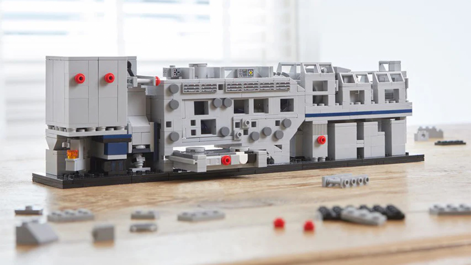
A Lego version of an ASML Lithography machine. (Image credit: ASML)
To eliminate the need for stitching, the industry is exploring larger orthogonal 6×12-inch photomasks to compensate for anamorphic optics. By doubling the reticle dimension corresponding to High-NA's 8X reduction direction, these masks are set to restore the traditional 26×33 mm full exposure field and enable even reticle-sized dies to be patterned without stitching.
However, 6×6-inch photomasks have been an industry standard for around three decades since the 1990s. Even the transition from DUV to EUV did not change the basic mask dimensions: EUV replaced transmissive masks with reflective multilayer masks but retained the 6×6-inch substrate form factor. As a result, the adoption of 6×12-inch reticles would require the industry to change the entire mask-making, mask handling, and lithography infrastructure built around the existing format.
Mask-blank suppliers like AGC and Hoya would need new or modified equipment to produce larger substrates and deposit uniform reflective EUV multilayers across a much larger area. Mask shops would need new or modified writers and etch tools to pattern the larger masks, as well as inspection and metrology systems capable of precise characterization of the new format. Cleaning equipment, pellicles, and pellicle-mounting devices would also require modifications.
The mask handling infrastructure would have to change as well. Suppliers would need larger mask pods, while fabs and mask shops would require compatible storage, transport, and automated handling systems. At the same time, they would have to retain support for existing 6×6-inch masks since existing and future Low-NA EUV and DUV scanners will continue to use the established format.
Perhaps the biggest changes would be required from ASML. Its High-NA EUV scanners would need modifications or a redesign to accept, clamp, move, and position the substantially larger reticles with the extreme precision required for EUV lithography.
Intel, Micron, Samsung, SK hynix, TSMC, and other chipmakers planning to adopt High-NA EUV lithography would then have to qualify the new masks, scanners, and other tools for their process flows and ensure that the full-field exposure capability works as intended.
As a result, the adoption of 6×12-inch masks would require a coordinated effort and significant investments from chipmakers, ASML, mask makers, and numerous equipment and materials suppliers.
To make matters more complicated, 6×12-inch masks will not replace the existing 6×6-inch format altogether, as noted above. The industry would therefore have to manufacture, inspect, transport, store, and handle two mask formats in parallel, which will add cost and complexity to an already expensive transition.
Timeline
The transition to 6×12-inch reticles is an industry effort currently supported by ASML, Intel, Samsung, and TSMC. It is going to take years and will happen well after High-NA EUV enters high-volume manufacturing with today's 6×6-inch photomasks, as the semiconductor industry prefers to adopt new technologies gradually.
Intel already uses High-NA EUV scanner(s) for select Intel 18A layers (patterned at Fab D1X) and supports both floorplanning within the half-field and stitching; Samsung plans to introduce High-NA EUV into DRAM high-volume manufacturing by 2028, and TSMC intends to deploy the technology for advanced-node production starting in 2030. All three companies plan to start High-NA EUV adoption with 6×6-inch masks.
Intel seems to be leading the pack with 6×12-inch reticles as it has been working for three years to make them a reality, but the company remains tight-lipped about the timing of its adoption of the new photomasks. Meanwhile, the ASML-TSMC initiative targets a 6×12-inch photomask pilot line by 2031, which should provide the foundry with a platform to develop and qualify the new mask format and associated manufacturing infrastructure. The ultimate target is full lithography-system readiness for advanced-node production by 2033.
That said, 6×6-inch and 6×12-inch photomasks for High-NA EUV patterning will likely co-exist on the market at least for some time rather than undergo an abrupt transition. At the end of the day, square 6×6-inch reticles that enable High-NA EUV scanners to expose fields as large as 26×16.5 mm (or 429 mm²) should be sufficient for the vast majority of client processors produced in the coming years. Larger 6×12-inch masks will matter primarily for much bigger designs, such as high-end AI accelerators, data center CPUs, DPUs, high-end GPUs, and FPGAs, where the ability to expose a full 26×33 mm field without stitching becomes considerably more valuable.
Anton Shilov is a contributing writer at Tom’s Hardware. Over the past couple of decades, he has covered everything from CPUs and GPUs to supercomputers and from modern process technologies and latest fab tools to high-tech industry trends.


 (Image credit: ASML)
 Like
0
Like
0
 Dislike
0
Dislike
0
 Love
0
Love
0
 Funny
0
Funny
0
 Wow
0
Wow
0
 Sad
0
Sad
0
 Angry
0
Angry
0










Comments (0)