Imec's 2026 roadmap details 0.3nm nodes by 2038, CFET transistors become viable at 0.7nm — company redefines Moore's Law as cell sizes gain importance for density
Jun 29, 2026 - 19:10
02
(Image credit: Imec)
Imec's semiconductor process technology roadmap sets the general direction of industry development and showcases the challenges the sector is set to face over the next few decades. The roadmap gives us an idea of the timelines for the next major process nodes and transistor architectures the company will research and develop in cooperation with industry giants, such as TSMC, Intel, Nvidia, AMD, Samsung, and ASML, among many others.
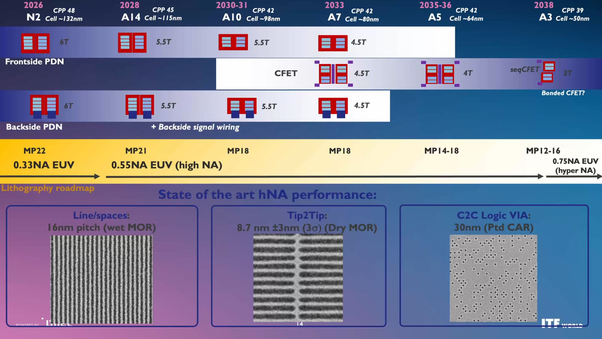
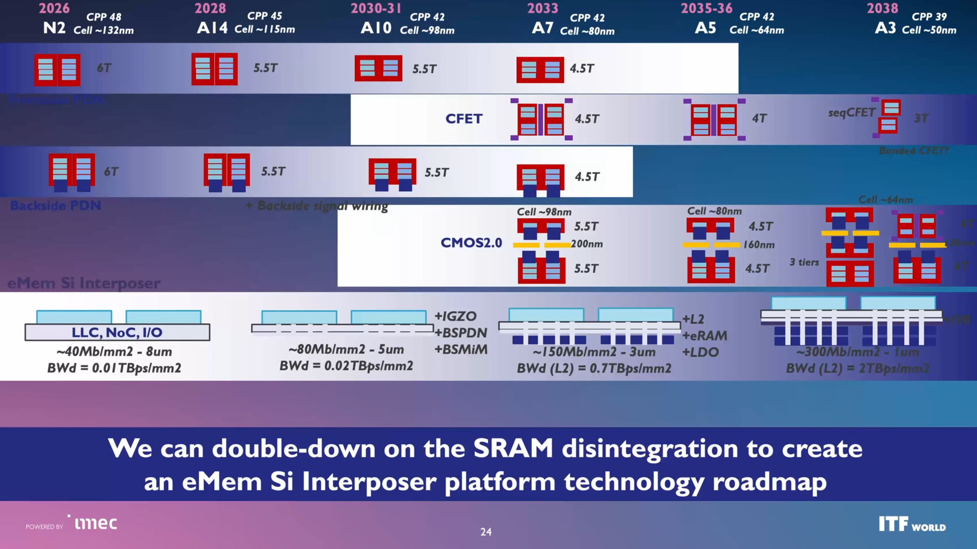
Imec's latest production node roadmap shows that the international research and development organization envisions 3 angstrom-class (0.3nm) fabrication technologies by 2038, but expects contact poly pitch (CPP) to stop scaling at A10 in 2030. While things might not be looking great for Moore's Law for imec, to continue scaling the chipmaker will need to adopt new technologies, such as CFET transistors and likely Hyper-NA EUV Lithography systems.
GAA transistors have seven years left
As the production of semiconductors becomes substantially more complicated, chipmakers no longer introduce all-new process technologies every couple of years. Instead, they typically roll out a new node generation every three years, with annual incremental enhancements in between. TSMC ramped N3B production in 2023, then followed it up with N3E in 2024, and N3P in 2025. Intel planned to follow the same pattern with 20A in 2024 (which was canceled), 18A in 2025, and 18A-P in 2027.
Next-generation process technologies will continue to emerge at similar cadences, according to imec's roadmap.
(Image credit: Imec)
Interuniversity Microelectronics Centre considers that we now live in the 2nm-class era (N2) with contact poly pitch (CPP) of around 48nm, as well as cell height of around 132nm and 6 metal tracks. The reality may be a bit different as Intel's 18A has a CPP of 50nm as well as a cell height of 160nm (high density) or 190nm (high performance), whereas TSMC's N3 can boast with a CPP of 45nm. N2 (or 18A, if you wish) will be followed by its performance and efficiency-enhanced version in the next couple of years, which is in line with how the industry has been operating in recent years.
"Of course, we are going to extend our logic roadmap to the next generation beyond N2," said Julien Ryckaert, vice president of R&D at imec. "As you know, in two nanometers we have already jumped into a new technology device paradigm in the nanosheet era, and that is going to bring us deep into the Angstrom node."
(Image credit: Imec)
Imec expects the A14-class to emerge in 2028. TSMC expects to start high-volume manufacturing using A14 in late 2028, so the actual ramp will happen in 2029. Intel's 14A follows the same pattern. With A14, imec projects CPP to shrink to 45nm and cell height to drop to 115nm and 5.5 metal tracks. Around 2030–2031, imec expects an A10-class technology — or a 1nm-class — with a 42 nm CPP and 98 nm cell height, which will still rely on a 5.5-track architecture.
It is noteworthy that gate-all-around (GAA) transistor-based nodes can be implemented either with conventional frontside power delivery networks or with backside power delivery, which reflects both imec's and TSMC's belief that BSPDN will not immediately become mandatory across all applications, as many of them do not benefit from it.
It is also worth mentioning that imec expects High-NA EUV tools insertion at A14, which is in line with Intel's plans, but not with TSMC's plans.
CFET insertion in the early 2030s
The roadmap becomes particularly interesting at the A7 generation, which imec expects to come in 2033. While CPP remains at 42 nm, cell height drops to roughly 80nm, and the standard-cell architecture moves to 4.5 tracks. More importantly, A7 is the point where CFET emerges as a serious candidate for production insertion. Instead of placing n-type and p-type transistors side by side, CFET stacks them vertically, which adds a third dimension to transistor scaling.
Imec’s roadmap explicitly positions CFET as the leading contender for A7, which means that the organization sees conventional nanosheet architectures approaching practical scaling limits in the early 2030s. Yet, since A7's CPP does not change from A10, chipmakers may or may not adopt the all-new transistor architecture at A7. Also note that imec seems to consider BSPDN as mandatory for CFETs.
(Image credit: Imec)
"Moving into A7, the seventh-angstrom generation, which is the fourth generation of nanosheet, we see more and more challenges in scaling the conventional nanosheet device technology," Ryckaert said. "There is a contender that we have already mentioned as well in previous presentations, where CFET could start emerging as the solution for the next era of transistors."
Beyond A7, the roadmap seems to depend on CFET evolution. The A5 generation, expected in 2035–2036, retains a 42nm CPP but reduces cell height to about 64nm using a 4-track library. By 2038, the roadmap reaches A3 with a 39nm CPP and 50nm cell height. At this point, imec envisions sequential CFET implementations and eventually bonded CFET structures that further exploit vertical integration. In fact, vertical integration seems to be the new way we should look at Moore's Law's evolution. Meanwhile, to get to a 39nm CPP and 50nm cell height, chipmakers might need to use Hyper-NA EUV lithography scanners, according to imec.
Redefining Moore's Law
(Image credit: Imec)
The most interesting thing about imec's roadmap is that it essentially redefines what Moore's Law means. Traditionally, we consider Moore's Law as the observation that the number of transistors on a chip of a certain size doubles every 18 – 24 months, as they are getting smaller.
The fact that imec shows CPP stuck at 42 nm from A10 through A5 is almost an admission that classical transistor scaling is running out of steam, and future density gains must come from vertical integration. In the imec roadmap, transistors are still getting denser, but not exactly because individual transistors are shrinking at the same pace they used to decades ago, but because chip designers can fit more logic gates into a given area because of different transistor architectures, 3D integration, or backside power delivery.
As a result, in the coming years, we may no longer care how many nanometers a gate pitch is, or individual transistors, but rather the size of a standard cell. After all, when companies like AMD, Intel, or Nvidia design a chip, they do not place individual transistors, but actual blocks built from standard cells. Yet, calculating the size of a standard cell is complicated because while cell height is fixed, its width is not, and depends on the actual function.
Library height × CPP is not the size of a specific standard cell. It is the fundamental footprint unit of a standard-cell library and a widely used proxy for logic density. Actual standard cells have that height, but their width varies depending on function. Instead, the industry uses such metrics as logic cell area (standard-cell footprint) — Cell Height × CPP — that measures the actual footprint of the logic building blocks that designers use, not just the dimensions of individual transistors.
The transition from 6-track cells at N2 to 3-track cells at A3 illustrates how future density gains will rely as much on shrinking standard-cell height as on reducing transistor pitch. As a result, despite the fact that CPP shrinkage is expected to stall for years, logic cell area is set to decrease; designers will be able to extract transistor density gain from future nodes, proving that Moore's Law is still here.
Given all the changes that the semiconductor industry is already experiencing and what is set to come, imec believes the sector is entering a new era that it calls Heterogeneous Large-Scale Integration (HLSI). The concept reflects a shift away from traditional VLSI scaling, where progress largely depended on the evolution of transistors and increasing transistor density, toward a model that combines multiple technologies within a single compute platform.
Future systems will rely on heterogeneous integration of logic, memory, power-delivery circuitry, and optical I/O using advanced 3D and 3D + 2.5D packaging technologies, according to imec's predictions. Of course, the organization expects AI workloads to become the main driver of semiconductor demand, so expect both compute architectures and the semiconductor industry to evolve in a direction that satisfies the needs of AI applications.
"As we will move deeper into AI-driven architecture, we will need to double down on the heterogeneity that technology offers, and this will probably move the VLSI paradigm to the HLSI paradigm, the Heterogeneous Large Scale Integration," Ryckaert said.
To optimize future platforms on the system level rather than develop individual components in isolation, imec has established its Cross-Technology Co-Optimization (XTCO) framework, which could be seen as an integral part of the HLSI vision. XTCO is designed to wed development logic, memory, interconnects, power delivery, cooling, and packaging, and assesses their impact on key system metrics such as compute density, energy efficiency, thermal performance, and memory.
It remains to be seen how this is going to work out, if at all, given the fact that logic process technologies are developed at foundries, memory technologies are designed at DRAM makers, whereas cooling is developed at third parties like CoolIt or Frore Systems.
Power and cooling
As individual chips get denser and more power-hungry, power delivery is set to become a critical bottleneck, which is why all leading chipmakers — Intel, Samsung, and TSMC — are implementing or set to implement backside power delivery technologies and integrated voltage regulators.
Imec expects future AI accelerators and CPUs to rely on a combination of BSPDN, IVRs, embedded capacitors, and advanced power semiconductors to reduce losses and improve efficiency. Over time, more power-conversion stages are expected to migrate from racks and motherboards into packages themselves to deliver cleaner power directly to transistors.
Since we are talking about multi-chiplet packages consuming kilowatts of power, the importance of cooling is hard to overestimate. For sure, 3D stacking and CFETs will not make cooling any easier because thermal power density is set to increase linearly with the number of transistors, thermal resistance is set to increase, and local hotspots will become an even bigger problem than they are today. As a result, imec expects future compute platforms to rely on a combination of more advanced cooling technologies, improved heat spreading, fine-grained thermal sensors, and system-level thermal optimization techniques.
"At the end of the day, what we need to achieve is a reduced energy cost of data movement. We need to improve the TDP for better thermal management," Ryckaert said. "We need to improve the efficiency of the power delivery, and we need to obviously increase the compute density to improve the functionality."
In short, useful future scaling will depend not only on the ability to build transistors and increase their density, but on delivering power efficiently and removing heat effectively.
Paving the path forward
Imec's latest semiconductor roadmap projects logic process technologies all the way to A3 generation around 2038 and argues that Moore's Law can continue despite the slowing pace of traditional transistor scaling. While the Dennard scaling for semiconductors is over, there are plenty of interesting things incoming.
According to the roadmap, conventional gate-all-around nanosheet transistors should remain viable through A10, while CFET architectures become a candidate for production insertion at the A7 generation around 2033. Meanwhile, future transistor density gains are expected to come from vertical integration, reduced standard-cell footprints, and eventually sequential and bonded CFET structures rather than from aggressive shrinking of transistor dimensions.
Anton Shilov is a contributing writer at Tom’s Hardware. Over the past couple of decades, he has covered everything from CPUs and GPUs to supercomputers and from modern process technologies and latest fab tools to high-tech industry trends.
 (Image credit: Imec)
 Like
0
Like
0
 Dislike
0
Dislike
0
 Love
0
Love
0
 Funny
0
Funny
0
 Wow
0
Wow
0
 Sad
0
Sad
0
 Angry
0
Angry
0


Comments (0)